Bloch surface plasmon optical device for enhancing Goos-Hanchen effect of graphene

An optical device and graphene technology, applied in the field of optics, can solve the problem of small Goose-Hanchen displacement of graphene, and achieve the effect of enhancing the Goose-Hanchen displacement effect and achieving compatibility

Active Publication Date: 2020-08-07
TIANJIN UNIV OF TECH & EDUCATION TEACHER DEV CENT OF CHINA VOCATIONAL TRAINING & GUIDANCE
View PDF3 Cites 0 Cited by
  • Summary
  • Abstract
  • Description
  • Claims
  • Application Information

AI Technical Summary

Problems solved by technology

[0004] The purpose of the present invention is to solve the problem that the graphene Goos-Hanchen shift is smaller in the existing structure, and to provide a Bloch surface polar optical device that significantly enhances the graphene Goos-Hanchen effect

Method used


Image

  • Bloch surface plasmon optical device for enhancing Goos-Hanchen effect of graphene
  • Bloch surface plasmon optical device for enhancing Goos-Hanchen effect of graphene
  • Bloch surface plasmon optical device for enhancing Goos-Hanchen effect of graphene

Examples


Embodiment 1

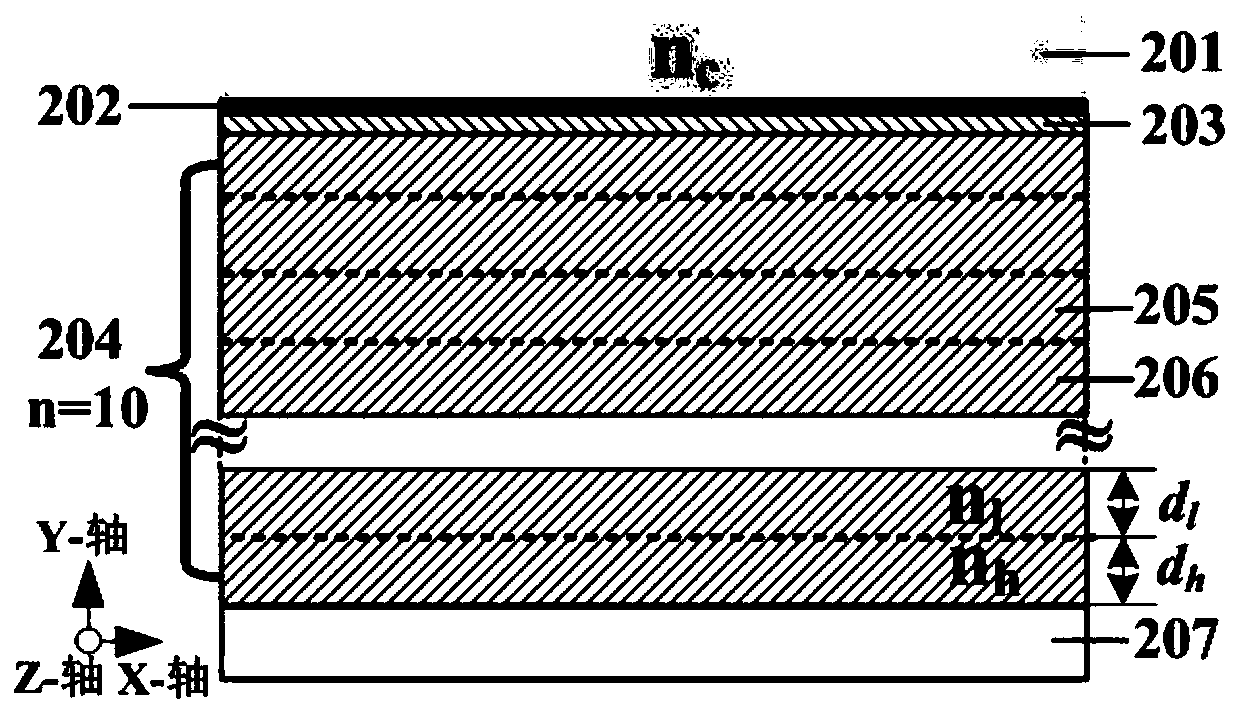
[0058] Embodiment 1, the Bloch surface polar optical device of 10 periodic multilayer dielectric material layers

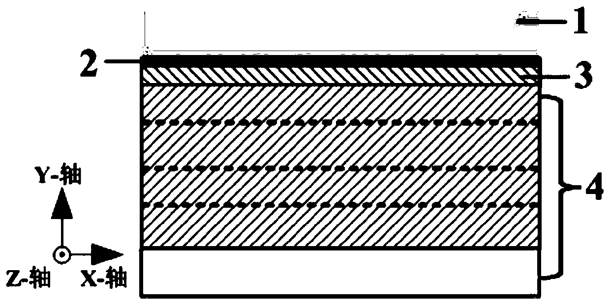
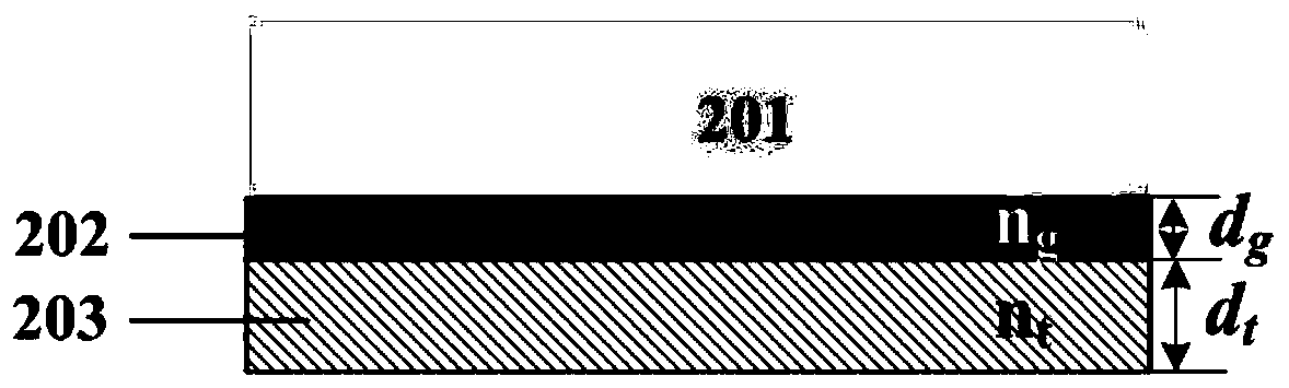
[0059] figure 2 It is a structural schematic diagram of the Bloch surface polariton optical device described in Example 1. image 3 is a partially enlarged view of the Bloch surface polaritonic optical device described in Example 1. 201 is cladding layer, n c Its refractive index; 202 is the graphene layer of defect layer, n g is its refractive index, d g Its thickness; 203 is the high refractive index dielectric cut-off layer of the defect layer, n t is its refractive index, d t Its thickness; 204 is the multilayer dielectric material layer of 10 periodic multilayer film structural elements; 205 is the low refractive index medium layer of the multilayer dielectric material layer of multilayer film structural element, n l is its refractive index, d l Its thickness; 206 is the high refractive index dielectric layer of the multilayer dielectric material laye...

Embodiment 2

[0067] Embodiment 2: Bloch surface polar optical device with 8 periodic multilayer dielectric material layers

[0068] Figure 8 It is a structural schematic diagram of the Bloch surface polariton optical device described in Example 2. Figure 9 is a partially enlarged view of the Bloch surface polaritonic optical device described in Example 2. 801 is the cladding layer, n c Its refractive index; 802 is the graphene layer of defect layer, n g is its refractive index, d g Its thickness; 803 is the high refractive index cut-off layer of the defect layer, n t is its refractive index, d t Its thickness; 804 is the multilayer dielectric material layer of 8 periodic multilayer film structural elements; 805 is the low refractive index medium layer of the multilayer dielectric material layer of multilayer film structural element, n l is its refractive index, d l Its thickness; 806 is the high refractive index medium layer of the multilayer dielectric material layer of the multi...


PUM

PropertyMeasurementUnit
Thicknessaaaaaaaaaa
Thicknessaaaaaaaaaa
Thickness rangeaaaaaaaaaa

Abstract

The invention discloses a Bloch surface plasmon optical device for enhancing the Goos-Hanchen effect of graphene. The cross section of the device comprises a coating layer, a graphene layer, a high-refractive-index medium cut-off layer and a multilayer film structure element; the refractive index or thickness of the coating layer or a certain layer of structure is adjusted; light input at a specific angle enters to the surface of the Bloch surface plasmon optical device; a remarkably enhanced light field is limited to the surface of graphene, so that interaction between the graphene and the light is enhanced, and Bloch surface plasmons are excited, violent jumping of a reflection phase is achieved, and therefore, the Goos-Hanchen shift effect on the surface of the graphene is remarkably enhanced. The optical device provided by the invention has very important significance for realizing the optical sensing detection of graphene in the potential application fields mainly including optical switches, optical storage and other photoelectric devices in optical communication and in the sensing field.

Description

technical field [0001] The invention relates to the field of optical technology, in particular to a Bloch surface excitation optical device that enhances the Gouss-Hanchen effect of graphene. Background technique [0002] When the light beam is reflected at the interface, when the reflectivity function (including intensity and phase) of the interface is not constant, a series of non-specular reflection phenomena may occur. For example: the beam center may have a certain lateral displacement between the incident point and the exit point of the reflective interface. This phenomenon was first confirmed by Goos and Hanchen through experiments, so it is called the Goos Hanchen effect. As a typical effect of non-specular reflection, the Goose-Hanchen phenomenon has become a research hotspot since its discovery, and has been studied in depth for decades. It is found that the Goose-Hanchen phenomenon is caused by the jump of the angle-dependent phase term in the reflectivity funct...

Claims


Application Information

Patent Timeline
IPC IPC(8): G02B5/00
CPCG02B5/008
Inventor 孔维敬孟范强倪晓昌
Owner TIANJIN UNIV OF TECH & EDUCATION TEACHER DEV CENT OF CHINA VOCATIONAL TRAINING & GUIDANCE
Why Eureka
Try Eureka