Supercharge Your Innovation With Domain-Expert AI Agents!

Display panel and preparation method thereof

A display panel and pixel definition layer technology, which is applied in semiconductor/solid-state device manufacturing, semiconductor devices, electrical components, etc., can solve the problem of reduced brightness and lifespan of luminescent materials, life limitation of luminescent materials of sub-pixels, and influence on the display effect of display panels, etc. problem, to reduce the difficulty and achieve the effect of mass production

Active Publication Date: 2020-08-11
SHENZHEN CHINA STAR OPTOELECTRONICS SEMICON DISPLAY TECH CO LTD
View PDF4 Cites 2 Cited by
  • Summary
  • Abstract
  • Description
  • Claims
  • Application Information

AI Technical Summary

Problems solved by technology

[0005] The embodiment of this application provides a display panel and its preparation method to solve the problem that the life of the luminescent material of the sub-pixel is limited in the existing display panel. After the display panel works for a period of time, the brightness and life of the luminescent material will decrease, which will affect the technical problem of the display effect of the display panel

Method used


Image

  • Display panel and preparation method thereof
  • Display panel and preparation method thereof
  • Display panel and preparation method thereof

Examples


Embodiment Construction

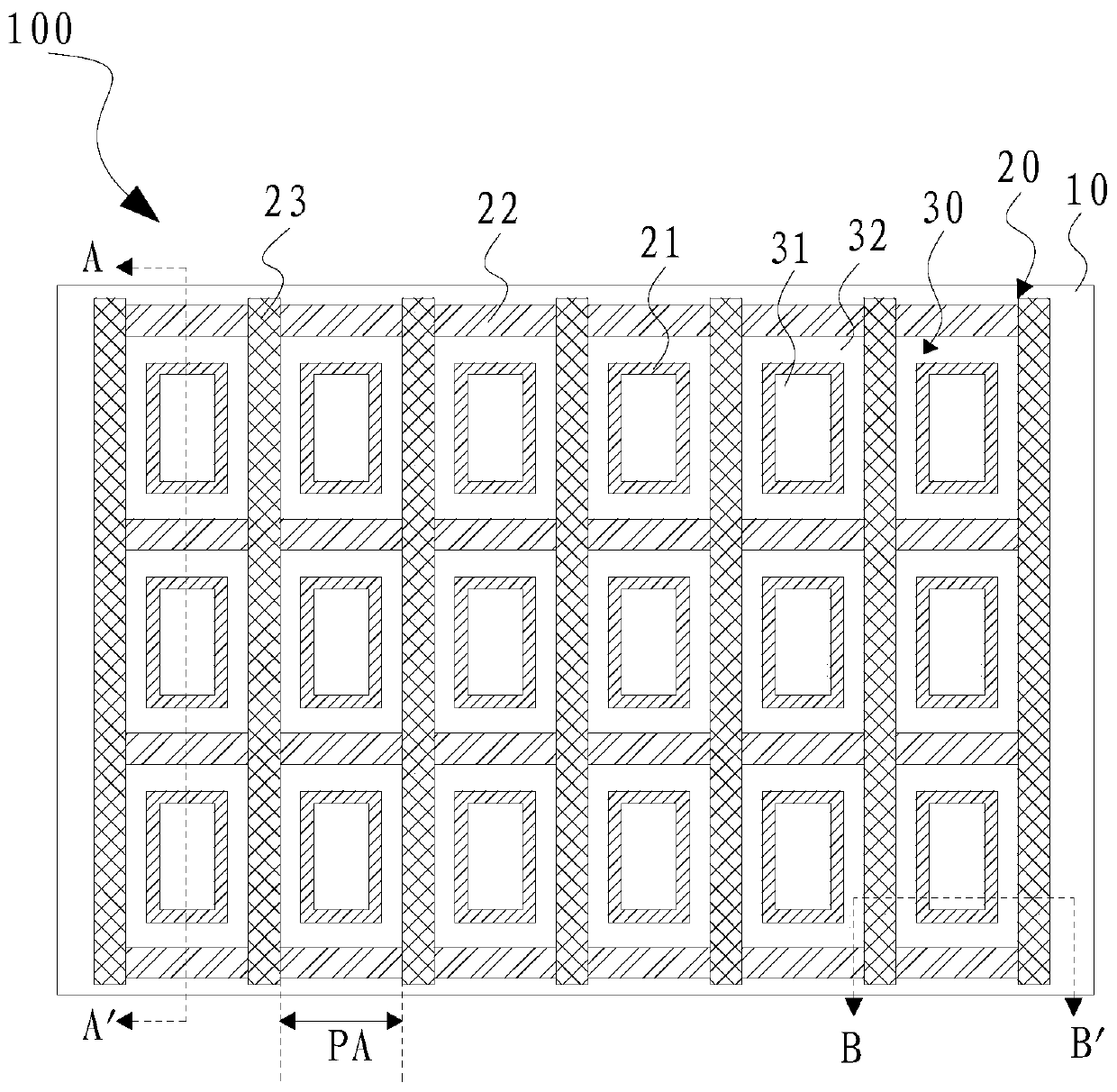
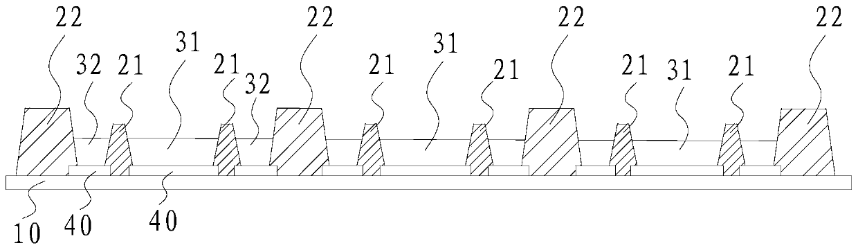
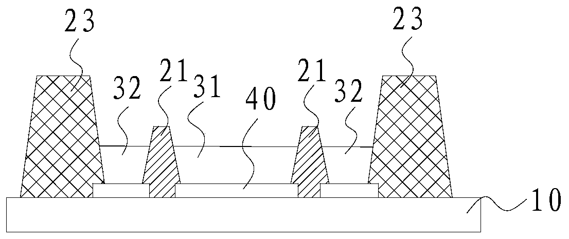
[0027] The technical solutions in the embodiments of the present application will be clearly and completely described below with reference to the accompanying drawings in the embodiments of the present application. Obviously, the described embodiments are only a part of the embodiments of the present application, but not all of the embodiments. Based on the embodiments in the present application, all other embodiments obtained by those skilled in the art without creative work fall within the protection scope of the present application.

[0028] In the description of this application, it should be understood that the terms "center", "longitudinal", "lateral", "length", "width", "thickness", "upper", "lower", "front", " rear, left, right, vertical, horizontal, top, bottom, inside, outside, clockwise, counterclockwise, etc., or The positional relationship is based on the orientation or positional relationship shown in the accompanying drawings, which is only for the convenience ...


PUM


Abstract

A display panel comprises a substrate, pixel definition layers and a plurality of sub-pixels, the pixel definition layers define a plurality of sub-pixel areas, the sub-pixels are arranged in the sub-pixel areas in a one-to-one correspondence mode, the sub-pixels comprise main pixels and sub-pixels surrounding the main pixels, and the main pixels and the sub-pixels are independently driven by different driving circuits respectively. The sub-pixels are designed into the main pixels and the sub-pixels surrounding the main pixels, and the main pixels and the sub-pixels are independently driven respectively, so that the brightness of the sub-pixels is favorably adjusted, and the light-emitting service life of the sub-pixels is favorably compensated; besides, by arranging the three pixel definition layers and controlling the heights and the material types of the three pixel definition layers, the printing difficulty of the light-emitting material can be reduced, and therefore mass production of products can be achieved.

Description

technical field [0001] The present application relates to the field of display technology, and in particular, to a display panel and a manufacturing method thereof. Background technique [0002] Organic electroluminescent display (Organic Light Emitting Display, OLED) is a new generation of display, OLED device usually includes a cathode, an anode, an organic thin film sandwiched between the cathode and the anode, after a voltage is applied between the cathode and the anode, the Organic thin films emit light. Compared with liquid crystal displays, OLED displays have many advantages such as self-illumination, fast response, wide viewing angle, and color saturation. [0003] Printed organic electroluminescence display (OLED) is a display technology that combines modern printing process with OLED display. It has the advantages of simple process, high material utilization, low cost, environmental protection, flexibility, etc. mainstream technology. Since the lifespan of the l...

Claims


Application Information

Patent Timeline
Patent Type & Authority Applications(China)
IPC IPC(8): H01L27/32H01L21/77
CPCH10K59/353H10K59/122H10K59/1201
Inventor 魏锋李金川
Owner SHENZHEN CHINA STAR OPTOELECTRONICS SEMICON DISPLAY TECH CO LTD
Features
  • R&D
  • Intellectual Property
  • Life Sciences
  • Materials
  • Tech Scout
  • Unparalleled Data Quality
  • Higher Quality Content
  • 60% Fewer Hallucinations
Learn More