A Broadband and Low Eddy Current Loss Artificial Conductor

An eddy current loss and artificial technology, applied in the direction of semiconductor devices, semiconductor/solid-state device parts, magnetic objects, etc., can solve the problem of narrow suppression frequency band and achieve the effect of solving the problem of narrow suppression frequency band and great application prospects

Active Publication Date: 2021-09-24
UNIV OF ELECTRONICS SCI & TECH OF CHINA
View PDF4 Cites 0 Cited by
  • Summary
  • Abstract
  • Description
  • Claims
  • Application Information

AI Technical Summary

Problems solved by technology

Effectively solve the problem of narrow suppression frequency band under low-frequency compensation encountered by FM / Cu (ferromagnetic layer / copper layer) multilayer film structure RF interconnection lines

Method used


Image

  • A Broadband and Low Eddy Current Loss Artificial Conductor
  • A Broadband and Low Eddy Current Loss Artificial Conductor
  • A Broadband and Low Eddy Current Loss Artificial Conductor

Examples


Embodiment 1

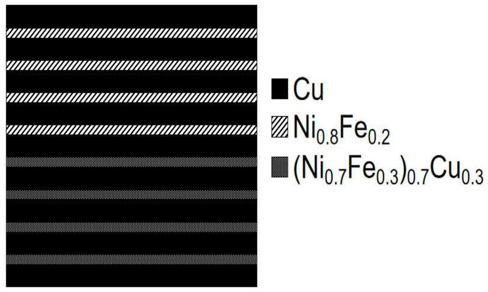
[0034] The artificial conductor structure of this embodiment is Cu / (Ni 0.7 Fe 0.3 ) 0.7 Cu 0.3 / Cu / (Ni 0.7 Fe 0.3 ) 0.7 Cu 0.3 / Cu / (Ni 0.7 Fe 0.3 ) 0.7 Cu 0.3 / Cu / (Ni 0.7 Fe 0.3 ) 0.7 Cu 0.3 / Cu / Ni 0.8 Fe 0.2 / Cu / Ni 0.8 Fe 0.2 / Cu / Ni 0.8 Fe 0.2 / Cu / Ni 0.8 Fe 0.2 / Cu, such as figure 1 shown. Among them, the Cu layer thickness is 500nm, the ferromagnetic layer thickness is 50nm (Cu has 9 layers, (Ni 0.7 Fe 0.3 ) 0.7 Cu 0.3 and Ni 0.8 Fe 0.2 4 layers each), with a total thickness of 4.9 μm. Among them, (Ni 0.7 Fe 0.3 ) 0.7 Cu 0.3 The magnetic film has low coercive force (Hce=3.26Oe, Hch=2.15Oe), natural resonance frequency is 491.1MHz, dynamic saturation magnetization is 5.77kGs, and damping factor is 0.026.

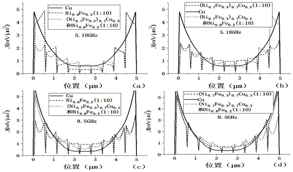
[0035] The structural parameters of the coplanar waveguide are set as follows: the base material is high-resistance silicon, the thickness is 0.15 mm, the width of the central conduction band is 15 μm, the total thickness of the conductor i...

Embodiment 2

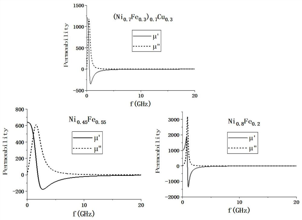
[0044] Compared with Embodiment 1, this embodiment differs in that: the artificial conductor structure is Cu / Ni from top to bottom 0.45 Fe 0.55 / Cu / Ni 0.45 Fe 0.55 / Cu / Ni 0.45 Fe 0.55 / Cu / Ni 0.45 Fe 0.55 / Cu / Ni 0.8 Fe 0.2 / Cu / Ni 0.8 Fe 0.2 / Cu / Ni 0.8 Fe 0.2 / Cu / Ni 0.8 Fe 0.2 / Cu, wherein, the Cu layer thickness is 500nm, the ferromagnetic layer thickness is 50nm (Cu has 9 layers, Ni 0.45 Fe 0.55 and Ni 0.8 Fe 0.2 4 layers each), with a total thickness of 4.9 μm. For Ni in the second half 0.8 Fe 0.2 , the compensation frequency point under this structure is 8.5GHz, and for the upper part of Ni 0.45 Fe 0.55 , the compensation frequency point is 14.3GHz.

[0045] Figure 5 The artificial conductor (Ni 0.45 Fe 0.55 and Ni 0.8 Fe 0.2 ) of the resistance value as a function of frequency, and compared it with a pure copper wire (Cu), using a ferromagnetic material as the magnetic layer (Ni 0.8 Fe 0.2 ), using a ferromagnetic material as the magnetic layer ...


PUM

PropertyMeasurementUnit
thicknessaaaaaaaaaa
thicknessaaaaaaaaaa
thicknessaaaaaaaaaa

Abstract

The invention relates to an artificial conductor with broadband and low eddy current loss, which belongs to the technical field of radio frequency devices and integrated circuits. The artificial conductor is a metal thin film layer / (ferromagnetic thin film layer / metal thin film layer) formed by alternate lamination of metal thin film layers and ferromagnetic thin film layers n The periodic multilayer film structure, wherein, the material of the 1st~n / 2 ferromagnetic thin film layer is ferromagnetic material A, and the material of (n / 2+1)~n ferromagnetic thin film layer is ferromagnetic material b. The invention adopts two different ferromagnetic materials as the ferromagnetic thin film layer to form an asymmetric structure, so that the artificial conductor can suppress eddy current loss in a wider frequency band. The artificial conductor of the present invention considers suppressing the eddy current loss at a lower frequency, and can also have an eddy current suppression effect in a wider frequency range, which solves the problem of narrow suppression frequency band under low frequency compensation, and has great advantages in radio frequency devices and integrated circuits. Great application prospects.

Description

technical field [0001] The invention relates to the technical field of radio frequency devices and integrated circuits, in particular to a wide-band low eddy current loss artificial conductor and a preparation method thereof, which can be applied to radio frequency devices and integrated circuits that need to work at higher frequencies and require low eddy current loss , such as coils of high-frequency inductors, and radio-frequency interconnections such as coplanar waveguides and microstrip lines. Background technique [0002] As the operating frequency of microelectronics and communication equipment continues to increase, one of the main disadvantages of integrated RF passive devices is that they are prone to significant eddy current losses. The eddy current effect at high frequencies is mainly affected by the skin effect, which not only causes RC delay, but also leads to poor quality factors and high power consumption of devices such as radio frequency inductors. People ...

Claims


Application Information

Patent Timeline
Patent Type & Authority Patents(China)
IPC IPC(8): H01F1/00H01F1/147H01L23/66C23C14/35C23C14/16C23C14/02
CPCC23C14/021C23C14/165C23C14/35H01F1/0027H01F1/147H01F1/14708H01L23/66
Inventor 白飞明黄铭贤金立川张怀武
Owner UNIV OF ELECTRONICS SCI & TECH OF CHINA
Why Eureka
Try Eureka