
Selective absorbing/emitting device construction method and system applicable to any wavelength

A technology of emission device and construction method, which is applied in the directions of instruments, optical components, optics, etc., can solve the problem of performance to be improved, and achieve the effect of high absorption characteristics

Active Publication Date: 2021-10-15
SHANGHAI JIAOTONG UNIV
View PDF5 Cites 0 Cited by
  • Summary
  • Abstract
  • Description
  • Claims
  • Application Information

AI Technical Summary

Problems solved by technology

The patent still needs to be improved in performance

Method used


Image

  • Selective absorbing/emitting device construction method and system applicable to any wavelength
  • Selective absorbing/emitting device construction method and system applicable to any wavelength
  • Selective absorbing/emitting device construction method and system applicable to any wavelength

Examples


Embodiment example 1

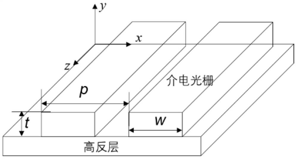
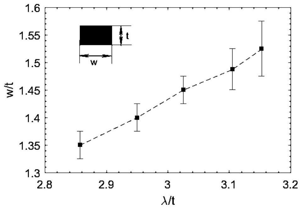
[0101] According to the dielectric grating selective absorption device design principle proposed by the present invention, when the thickness of the grating is set to be t=0.5 μm, the widths are respectively w=1.35t, 1.4t, 1.45t, 1.5t and 1.55t, and the period is p=w +0.07um, such as Figure 4 As shown, high absorption is achieved in the corresponding near-infrared bands. It should be pointed out that the target wavelength for achieving high absorption can be selected within the effective range proposed by the present invention according to actual needs.

Embodiment example 2

[0103] According to the dielectric grating selective absorption device design principle proposed by the present invention, the dielectric grating width w=1.35t is set, and the period is p=w+0.07um. Within the effective range proposed by the present invention, Figure 5 is the near-infrared absorption spectrum of the working band under different thickness t, Image 6 It is the absorption spectrum of the working band in the mid-infrared under different thickness t, and the near-perfect high absorption characteristics have been achieved in the corresponding bands. It should be pointed out that the target wavelength for achieving high absorption can be selected within the effective range proposed by the present invention according to actual needs.

[0104] Figure 7 Absorption spectra at different periods of the dielectric grating structure exemplified by the present invention when t=0.5um and w=1.45t. When the period changes between 0.78 μm and 0.98 μm, the change of the absorp...

Embodiment example 3

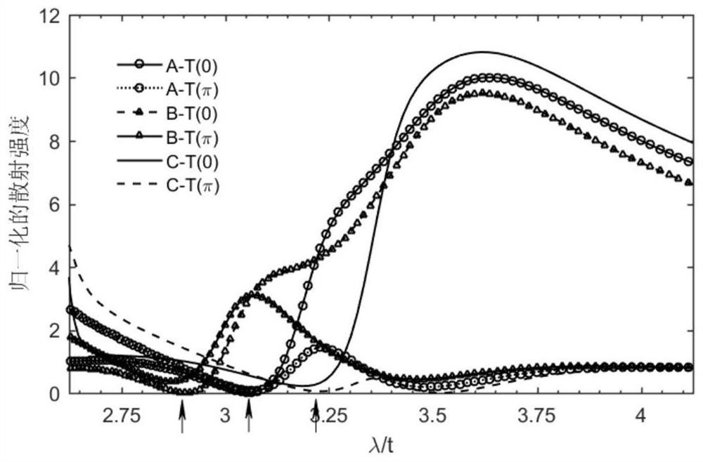
[0107] The components obtained according to the selective absorbing / emitting device design method applicable to any wavelength proposed by the invention can be further applied to the design and development of gas detection and refractive index detectors. Figure 9 For the dielectric grating structure t=0.5um of the present invention example, when w=1.45t, the absorption spectrum changes the spectrum with the background material refractive index, and its detection sensitivity (S=dλ / dn b , n b is the background refractive index) up to 350nm RIU -1 ,like Figure 10 .


PUM


Abstract

The present invention provides a method and system for constructing a selective absorption / emitting device suitable for any wavelength, including: step S1: constructing a sub-wavelength scale dielectric grating layer and a high-reflection base layer into a set structure; step S2: Select the geometric size of the dielectric grating, including the width w and the thickness t, to satisfy a certain multiple relationship; Step S3: move the period along the x direction, so that the incident light is p-polarized, the incident wave vector is along the negative direction of the y-axis, and the incident electric field E x Along the x direction, the incident magnetic field H z Along the z direction, where p is the period of the sub-wavelength scale grating structure; Step S4: Setting the structure can effectively concentrate the electromagnetic radiation energy in the grating plane. The invention solves the problems that the existing absorbing (emitting) devices rely on noble metal materials or multi-layer film structures in terms of cost and large scale.

Description

technical field [0001] The present invention relates to the technical field of selective absorption / emission devices, in particular to a method and system for constructing selective absorption / emission devices applicable to any wavelength. Background technique [0002] The design of selective emitter / absorber has a wide range of applications in solar cells, thermophotovoltaic, radiative cooling, gas detection, etc. In recent years, the rise of metamaterials and metasurfaces has provided a new platform for the design of high-performance absorbing / emitting devices. Researchers have focused on photonic crystals, multilayer film structures, and metal-dielectric-metal MIM structures. As well as hyperbolic metamaterials and even two-dimensional materials, perfect absorption at specific wavelengths can be achieved by exciting magnetic excitons, surface plasmons or surface phonon polaritons. Although the research on absorption / emitter has achieved certain results, it still faces so...

Claims


Application Information

Patent Timeline
Patent Type & Authority Patents(China)
IPC IPC(8): G02B27/00G02B5/00
CPCG02B5/003G02B27/0012
Inventor 赵长颖刘梦琦
Owner SHANGHAI JIAOTONG UNIV
Learn More