Eureka AIR delivers breakthrough ideas for toughest innovation challenges, trusted by R&D personnel around the world.

Manufacturing method of split-gate flash memory

A manufacturing method and memory technology, which are applied in semiconductor/solid-state device manufacturing, electrical solid-state devices, semiconductor devices, etc., can solve the problems of easy programming failure of semiconductor substrates

Pending Publication Date: 2020-09-01
SHANGHAI HUAHONG GRACE SEMICON MFG CORP
View PDF4 Cites 0 Cited by
  • Summary
  • Abstract
  • Description
  • Claims
  • Application Information

AI Technical Summary

Problems solved by technology

[0005] The invention provides a method for manufacturing split-gate flash memory, aiming to solve the problem that part of the semiconductor substrates in the same batch of semiconductor substrates undergoing a furnace tube process are prone to programming failure

Method used


Image

  • Manufacturing method of split-gate flash memory
  • Manufacturing method of split-gate flash memory
  • Manufacturing method of split-gate flash memory

Examples


Embodiment Construction

[0038] The manufacturing method of the split-gate flash memory proposed by the present invention will be further described in detail below in conjunction with the accompanying drawings and specific embodiments. The advantages and features of the present invention will become clearer from the following description. It should be noted that all the drawings are in a very simplified form and use imprecise scales, and are only used to facilitate and clearly assist the purpose of illustrating the embodiments of the present invention.

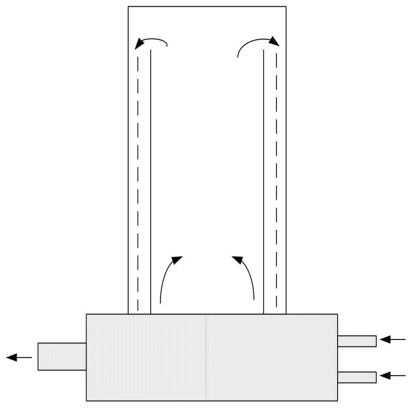
[0039] Before introducing the manufacturing method of the split-gate flash memory of the present invention, the characteristics of the furnace tube process are firstly introduced, so as to better understand the technical solution of the present invention.

[0040] At present, most of the furnace tubes used in the semiconductor industry are vertical, and they are divided into atmospheric pressure furnace tubes and low pressure furnace tubes according t...


PUM

PropertyMeasurementUnit
thicknessaaaaaaaaaa
thicknessaaaaaaaaaa

Abstract

The invention provides a manufacturing method of a split-gate flash memory. According to the manufacturing method, a side wall material layer used for manufacturing a first side wall on a floating gate and a tunneling oxide layer located between the floating gate and a word line are manufactured through a furnace tube technology, and the tunneling oxide layer is formed according to the sequence opposite to the sequence of all semiconductor substrates in a furnace tube cavity when the side wall material layer is formed. The problem that in the furnace tube technology, a substrate located at thetop in a furnace tube cavity is thinner than a substrate film layer at the bottom is solved. When the side wall material layer and the tunneling oxide layer are formed, the semiconductor substrates are arranged in the furnace tube cavity according to an opposite sequence, the thin side wall material layer is formed on the semiconductor substrate, and a thick tunneling oxide layer is formed on thesemiconductor substrate, the problem of programming failure caused by the fact that the side wall material layer and the tunneling oxide layer are both too thin can be avoided for the split-gate flash memory manufactured on the basis of each semiconductor substrate, and the production yield can be improved.

Description

technical field [0001] The invention relates to the technical field of semiconductors, in particular to a manufacturing method of a split-gate flash memory. Background technique [0002] In the current semiconductor industry, flash memory is divided into two types: stack gate flash memory and split gate flash memory. Although the method of manufacturing the stacked gate flash memory is simpler than that of the split gate flash memory, the stacked gate flash memory has the problem of over-erasing. The split-gate flash memory can effectively avoid over-erasing, and the circuit design is relatively simple. In addition, the split-gate flash memory uses source-side hot electron injection for programming, which has higher programming efficiency, and thus is widely used in various electronic products such as smart cards, SIM cards, microcontrollers, and mobile phones. [0003] An existing split-gate flash memory includes a semiconductor substrate, a floating gate, a floating gate...

Claims


Application Information

Patent Timeline
Patent Type & Authority Applications(China)
IPC IPC(8): H01L27/11521H01L21/336H10B41/30
CPCH01L29/66825H10B41/30
Inventor 汤志林王卉曹子贵
Owner SHANGHAI HUAHONG GRACE SEMICON MFG CORP
Why Eureka
Eureka Blog
Learn More