Analog voltage output circuit, analog voltage calculation method and sensor
A technology of analog voltage and output circuit, which is applied in the electronic field and can solve problems affecting sensor performance, low accuracy of analog voltage signals, and affecting the detection accuracy of pressure sensors, etc.
- Summary
- Abstract
- Description
- Claims
- Application Information
AI Technical Summary
Problems solved by technology
Method used
Image

Examples
Embodiment 1
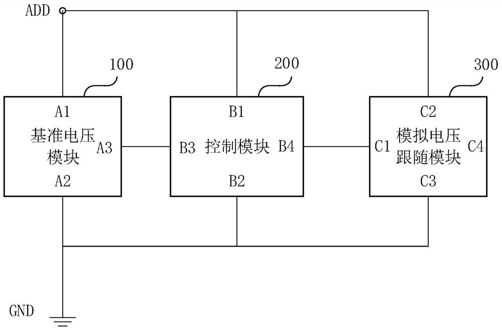
[0021] figure 1 For a schematic structural diagram of an analog voltage output circuit provided in Embodiment 1 of the present invention, refer to figure 1 , the analog voltage output circuit includes: a reference voltage module 100, a control module 200 and an analog voltage follower module 300;
[0022] The reference voltage module 100 includes a first power input terminal A1, a second power input terminal A2 and a reference voltage output terminal A3. The first power input terminal A1 of the reference voltage module 100 is connected to the first power supply signal ADD. The first power supply signal ADD of the reference voltage module 100 The second power supply input terminal A2 is connected to the second power supply signal GND; the reference voltage module 100 is used to provide the reference voltage to the control module 200;
[0023] The control module 200 includes a first power input terminal B1, a second power input terminal B2, a sampling voltage input terminal B3 ...
Embodiment 2
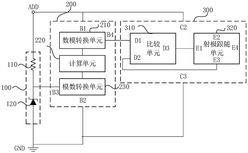
[0032] figure 2 It is a schematic structural diagram of an analog voltage output circuit provided in Embodiment 2 of the present invention. On the basis of Embodiment 1, refer to figure 2 , the reference voltage module further includes a Zener diode 120 and a first resistor 110;
[0033] The first end of the first resistor 110 is used as the first power supply input terminal A1 of the reference voltage module 100 to input the first power supply signal ADD, and the second end of the first resistor 110 is electrically connected to the cathode of the Zener diode 120;
[0034] The anode of the Zener diode 120 is connected to the second power signal GDN, and the anode of the Zener diode 120 is electrically connected to the second power input terminal A2 of the reference voltage module 100 and the second power input terminal B2 of the control module 200 respectively.
[0035] Among them, the Zener diode uses the reverse breakdown state of the pn junction, and its current can chan...
Embodiment 3
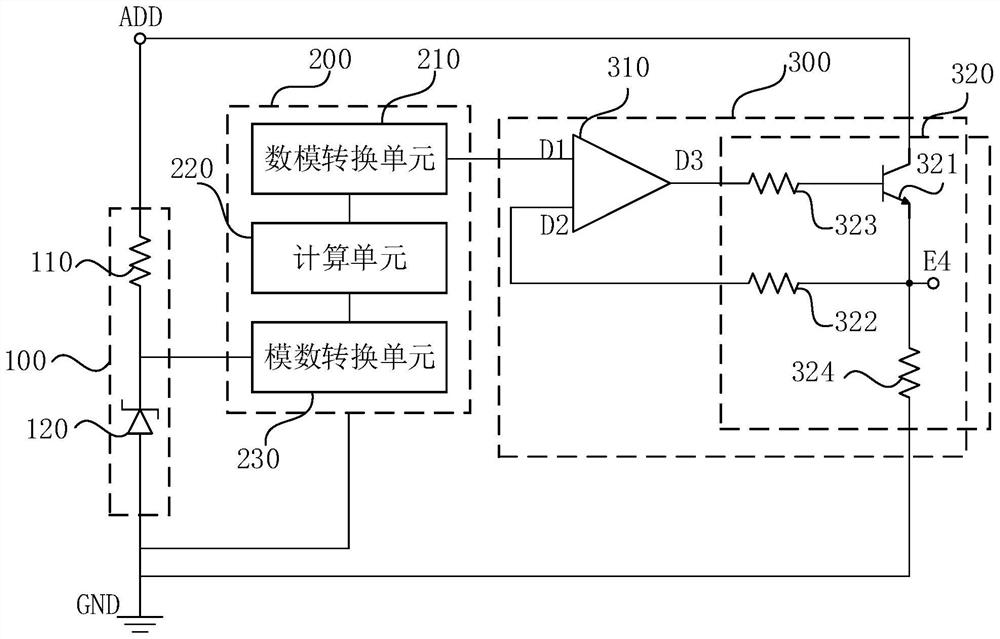
[0044] image 3 It is a schematic structural diagram of an analog voltage output circuit provided in Embodiment 3 of the present invention. On the basis of the above embodiments, refer to image 3 , the comparison unit is an operational amplifier.
[0045] refer to image 3 , the emitter follower unit 320 includes a triode 321, a second resistor 322, a third resistor 323 and a fourth resistor 324, the first input terminal D1 of the comparison unit 310 is electrically connected to the analog voltage output terminal B4 of the control module 200, the comparison unit 310 The second input terminal D2 of the second resistor 322 is electrically connected to the first terminal of the second resistor 322, the second terminal of the second resistor 322 is electrically connected to the analog voltage output terminal E4 of the analog voltage follower module 300, and the output terminal D3 of the comparison unit 310 is electrically connected to the first terminal of the second resistor 32...
PUM
 Abstract
Description
Claims
Application Information
 - R&D
- Intellectual Property
- Life Sciences
- Materials
- Tech Scout
- Unparalleled Data Quality
- Higher Quality Content
- 60% Fewer Hallucinations
Browse by: Latest US Patents, China's latest patents, Technical Efficacy Thesaurus, Application Domain, Technology Topic, Popular Technical Reports.
© 2025 PatSnap. All rights reserved.Legal|Privacy policy|Modern Slavery Act Transparency Statement|Sitemap|About US| Contact US: help@patsnap.com