Memory and forming method thereof

A memory and bit line technology, applied in the field of memory and its formation, can solve problems such as difficulty in balancing, and achieve the effect of increasing the size of the bottom and improving the transmission performance

Active Publication Date: 2020-09-08
FUJIAN JINHUA INTEGRATED CIRCUIT CO LTD
View PDF8 Cites 3 Cited by
  • Summary
  • Abstract
  • Description
  • Claims
  • Application Information

AI Technical Summary

Problems solved by technology

[0005] The purpose of the present invention is to provide a memory to solve the problem that the existing memory is diff

Method used


Image

  • Memory and forming method thereof
  • Memory and forming method thereof
  • Memory and forming method thereof

Examples


Embodiment 1

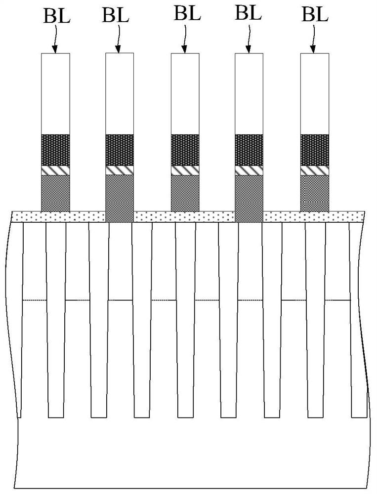
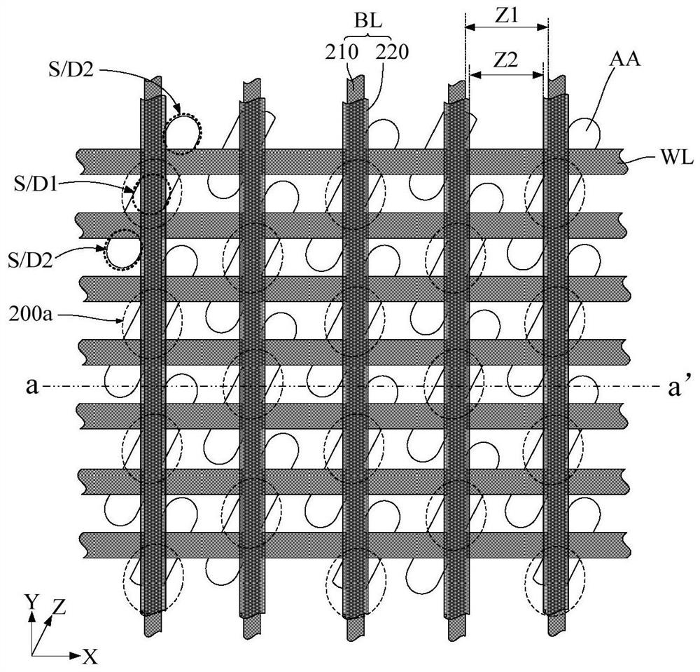
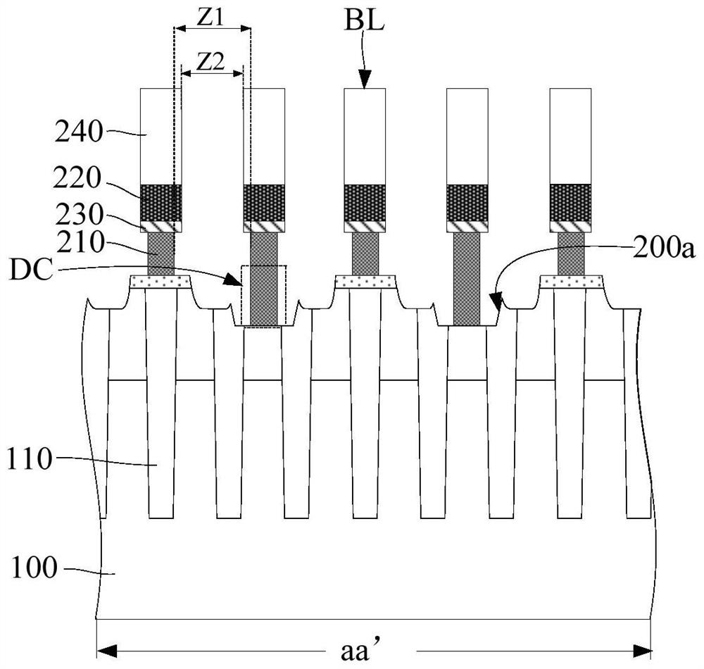
[0056] Figure 2a is a memory in Embodiment 1 of the present invention, which shows a top view of a bit line, Figure 2b for Figure 2a Shown is a schematic cross-sectional view of the memory in Embodiment 1 of the present invention along the aa' direction. It should be noted that, in order to illustrate the memory structure in this embodiment more clearly, Figure 2a The illustration of some components is omitted in , for example Figure 2a The substrate and part of the insulating layer etc. are not shown in the figure.

[0057] combine Figure 2a and Figure 2bAs shown, in this embodiment, the memory includes a substrate 100 and a bit line BL formed on the substrate 100, the bit line BL has a first conductive layer 210 and a second conductive layer 220, and the The width dimension of the first conductive layer 210 is smaller than the width dimension of the second conductive layer 220 above it.

[0058] Specifically, a plurality of active regions AA are formed in the s...

Embodiment 2

[0168] The difference from Embodiment 1 is that in the method for forming the memory of this embodiment, when performing the first etching process, the first etching process includes sequentially etching the second conductive material layer and the first conductive material layer, the side boundary of the first conductive material layer after the first etching process is flush with the side boundary of the second conductive layer; then, in the second etching process, the etchant only The sidewall of the first conductive material layer is etched downward to further reduce the size of the first conductive material layer laterally, so that the size of the formed first conductive layer is smaller than the size of the second conductive layer.

[0169] Figure 14 It is a schematic structural diagram of the formation method of the memory in Embodiment 2 of the present invention after the first etching process is performed.

[0170] specific reference Figure 14 As shown, when perform...


PUM


Abstract

The invention provides a memory and a forming method thereof. According to the bit lines in the memory, the width size of the first conductive layer is smaller than that of the second conductive layerabove the first conductive layer, so that the bottom interval size between the adjacent bit lines is larger than the top interval size of the adjacent bit lines. Thus, on the basis that the width size of the second conductive layer is met to guarantee the transmission performance of the bit lines, the bottom interval size between the adjacent bit lines is increased, and the bottom size of the storage node contact part filled between the adjacent bit lines can be further increased.

Description

technical field [0001] The invention relates to the technical field of semiconductors, in particular to a memory and a forming method thereof. Background technique [0002] A memory typically includes a storage capacitor for storing charge representing stored information and a storage transistor connected to the storage capacitor. Also, there are usually multiple word lines and bit lines in the memory for controlling selected memory transistors. [0003] figure 1 is a schematic diagram of the existing memory structure, such as figure 1 As shown, in the existing memory, the bit line BL includes a plurality of film layers stacked in sequence from bottom to top, and the width of each film layer is uniform. Specifically, when forming the bit line BL, it is based on the same mask pattern layer, and usually anisotropic etching process is used to etch each film layer, so that the pattern in the mask pattern layer can be accurately copied to each in the film layer. [0004] How...

Claims


Application Information

Patent Timeline
IPC IPC(8): H01L27/108H01L21/8242
CPCH10B99/00H10B12/30H10B12/485H10B12/482
Inventor 詹益旺黄永泰童宇诚朱贤士黄丰铭巫俊良
Owner FUJIAN JINHUA INTEGRATED CIRCUIT CO LTD
Why Eureka
Try Eureka