Electronic circuit
A technology for electronic circuits and printed wiring substrates, which is applied in the directions of printed circuits, printed circuits, and assembling printed circuits with electrical components, which can solve problems such as rising manufacturing costs of electronic circuits.
- Summary
- Abstract
- Description
- Claims
- Application Information
AI Technical Summary
Problems solved by technology
Method used
Image

Examples
no. 1 approach
[0026] [1-1. Overall structure]
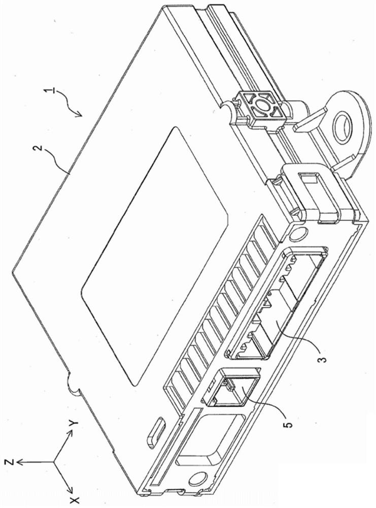
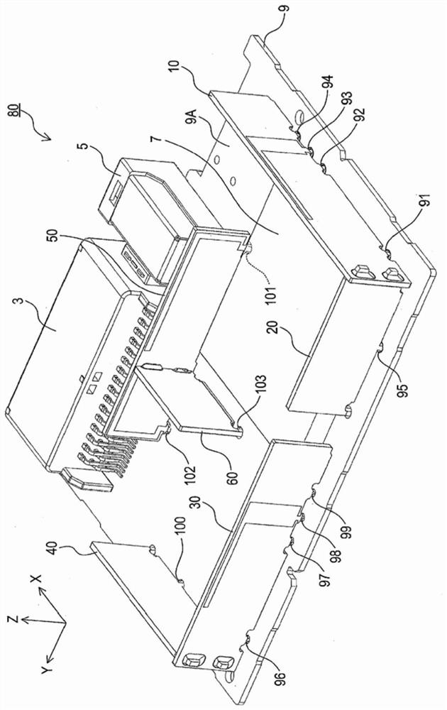
[0027] Such as figure 1 As shown, the antenna unit 1 in the first embodiment is a vehicle-mounted antenna unit, and includes a substantially rectangular parallelepiped housing 2 , and two connectors 3 and 5 are exposed from one side of the housing 2 . Such as figure 2 As shown, these two connectors 3 and 5 are surface-mounted (hereinafter, mounted) on a main substrate 9 by reflow soldering together with an IC chip 7 for performing various processes, and housed in a case 2 . In addition, six printed wiring boards 10 , 20 , 30 , 40 , 50 , and 60 , which are smaller than the printed wiring boards constituting the main board 9 , are mounted on the main board 9 by reflow soldering.
[0028] Furthermore, the main board 9 , the two connectors 3 and 5 mounted on the main board 9 , the IC chip 7 , and the six printed wiring boards 10 to 60 constitute an electronic circuit 80 as the first embodiment. In addition, in the following, the positional rel...
no. 2 approach
[0056] [2-1. Differences from the First Embodiment]
[0057] Since the second embodiment has the same basic configuration as that of the first embodiment, the description of the common configuration will be omitted, and the description will focus on the differences. The electronic circuit of the second embodiment is equipped with such Figure 9 The illustrated board pair including the printed wiring board 210 serving as the antenna board differs in points.
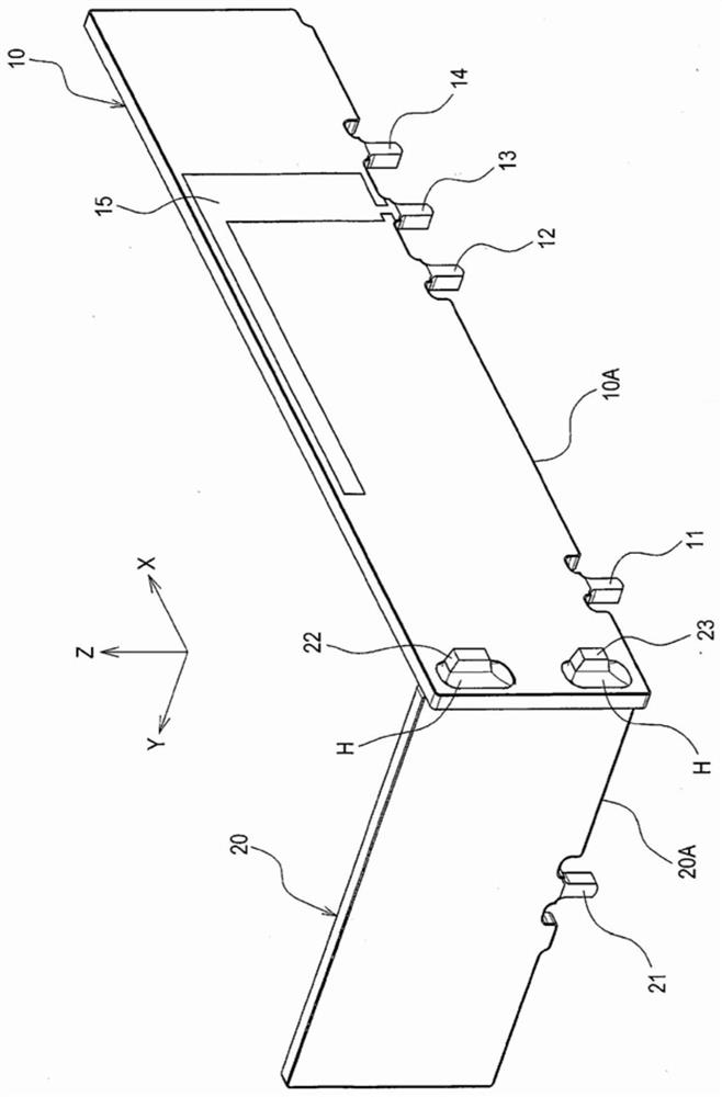
[0058] Such as Figure 9 As shown, printed wiring board 210 configured in a rectangular plate shape is mounted such that edge 210A corresponding to one long side of the rectangle abuts against component mounting surface 9A. Three protrusions 211 , 212 , and 213 protruding in the −Z direction are provided on the edge 210A. The protrusion 211 is configured to function as an electrode for feeding power to the antenna pattern 214 formed on the printed circuit board 210 . In addition, the protrusion 212 and the protrusion 2...
no. 3 approach
[0065] [3-1. Differences from the First Embodiment]
[0066] Since the third embodiment has the same basic configuration as that of the first embodiment, the description of the common configuration will be omitted, and the description will focus on different points. In the first embodiment, two rectangular through-holes 18 and 19 are formed in a line along the ±Z direction on the printed wiring board 10 serving as the antenna board. For this, the electronic circuit of the third embodiment is equipped with such Figure 10 The illustrated board pair including the printed wiring board 310 serving as the antenna board differs in points.
[0067] Such as Figure 10 As shown, the rectangular plate-shaped printed wiring board 310 is mounted such that an edge 310A corresponding to one long side of the rectangle abuts on the component mounting surface 9A. The edge 310A may be arranged in any direction on the component mounting surface 9A. However, similar to the printed circuit boar...
PUM
 Abstract
Description
Claims
Application Information
 - R&D
- Intellectual Property
- Life Sciences
- Materials
- Tech Scout
- Unparalleled Data Quality
- Higher Quality Content
- 60% Fewer Hallucinations
Browse by: Latest US Patents, China's latest patents, Technical Efficacy Thesaurus, Application Domain, Technology Topic, Popular Technical Reports.
© 2025 PatSnap. All rights reserved.Legal|Privacy policy|Modern Slavery Act Transparency Statement|Sitemap|About US| Contact US: help@patsnap.com