Mask structure of LCD display screen and manufacturing process thereof

A technology of LED display screen and manufacturing process, which is applied in the direction of instruments, identification devices, etc., to achieve the effect of reducing spacing, improving product reliability, and good picture quality

Inactive Publication Date: 2020-10-09
HEFEI PRECISE DISPLAY CO LTD
View PDF13 Cites 0 Cited by
  • Summary
  • Abstract
  • Description
  • Claims
  • Application Information

AI Technical Summary

Problems solved by technology

However, the problem of contrast in the prior art cannot be fundamentally solved through the visual sensory illusion effect

Method used


Image

  • Mask structure of LCD display screen and manufacturing process thereof
  • Mask structure of LCD display screen and manufacturing process thereof

Examples


Embodiment 1

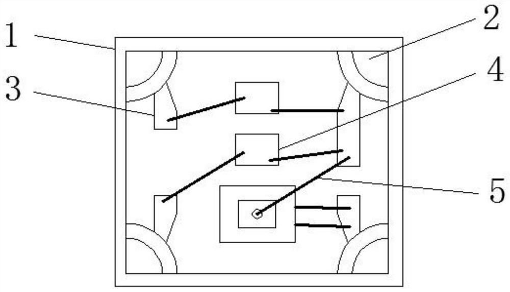
[0025] see figure 1 , in an embodiment of the present invention, a mask structure of an LCD display screen and its manufacturing process, the LED display screen is provided with a circuit cavity, the circuit cavity is provided with a circuit substrate 1, and the circuit substrate 1 is made of resin, Quartz and ceramics are made by mixing one or more of them. The upper and lower sides of the circuit substrate 1 are respectively provided with positive circuit lines and reverse circuit lines. The four corners of the circuit substrate 1 are all provided with wire holes 2. The wires of the positive circuit extend through the wire hole 2 and are connected to the reverse circuit, and the positive circuit is provided with a plurality of optical fixed sections 3 above, and ordinary light chips with different contrasts are respectively arranged in the fixed optical sections 3, The optical fixed sections 3 are respectively located on the sides of the wire holes 2, and the optical fixed s...

Embodiment 2

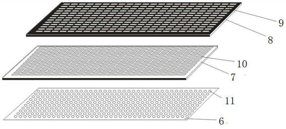
[0028] The present invention also provides a LED display screen string light surface treatment process. The outer casing of the LED display screen includes a press-fit plate and a mask. The mask is provided with several lines and is supported and fixed between adjacent press-fit plates. The surface treatment process includes the following steps:

[0029] The outer casing of the LED display screen includes a pressing plate 7 and a mask 8, the mask 8 is attached to the upper plane of the pressing plate 7, and the pressing plate 7 is provided with several light-transmitting holes 10, and the mask 8 is Several astigmatism holes 9 are provided, and the astigmatism holes 9 and the light transmission holes 10 are located on the same axis line, and the surface treatment process includes the following steps:

[0030] S1: Precision stamping: The press-fit plate 7 with high hardness is used, and the press-fit plate 7 and the mask 8 are pressed together by precision stamping; it is used t...


PUM

PropertyMeasurementUnit
thicknessaaaaaaaaaa

Abstract

The invention relates to the field of LED display screens. The invention relates to a mask structure, in particular to an LCD display screen mask structure and a manufacturing process thereof. An outer shell of the LED display screen comprises a pressing plate and a mask. The mask is attached to the upper plane of the pressing plate, a plurality of light transmitting holes are formed in the pressing plate, a plurality of light scattering holes are formed in the mask, the light scattering holes and the light transmitting holes are located on the same axis, and the surface treatment process comprises the following steps that S1, the pressing plate and the mask are subjected to pressing treatment in a precision stamping mode; S2, epoxy resin is filled; and S3, the mask is subjected to pressing treatment in a vacuum closed environment. According to the invention, through multi-line refraction of light, the light is uniformly mixed, and the emitted light has few mixed colors, so that the black and white contrast of the display screen is improved, and the brightness of the light is more uniform.

Description

technical field [0001] The invention relates to the field of LED display screens, in particular to a mask structure of an LCD display screen and a manufacturing process thereof. Background technique [0002] The LED display screen mask is of great significance for protecting the LED display screen. The existing LED display screen mask is formed by continuous splicing of multiple unit pieces, and pixels are evenly distributed on each unit piece; The splicing is prone to bulging, and the splicing gap is too large after being cold and black lines are easy to see; at the same time, the seam is also particularly obvious after splicing adjacent LED display modules; in addition, because the LED display mask is in production There is chromatic aberration, so continuous splicing in use will easily lead to uneven color on the surface of the LED display; in order to overcome the above difficulties, the existing LED display mask needs to be coated with glue on the back during production...

Claims


Application Information

Patent Timeline
Patent Type & Authority Applications(China)
IPC IPC(8): G09F9/33
CPCG09F9/33
Inventor 赵旭
Owner HEFEI PRECISE DISPLAY CO LTD
Why Eureka
Try Eureka