NOR-type memory device and method of fabricating the same

A technology of memory element and memory unit, which is applied in semiconductor/solid-state device manufacturing, static memory, digital memory information, etc.

Pending Publication Date: 2020-10-30
王振志 +1
View PDF8 Cites 0 Cited by
  • Summary
  • Abstract
  • Description
  • Claims
  • Application Information

AI Technical Summary

Problems solved by technology

However, 4F 2 The cell size is already the limit of these prior art NOR-type memory elements

Method used


Image

  • NOR-type memory device and method of fabricating the same
  • NOR-type memory device and method of fabricating the same
  • NOR-type memory device and method of fabricating the same

Examples


Embodiment Construction

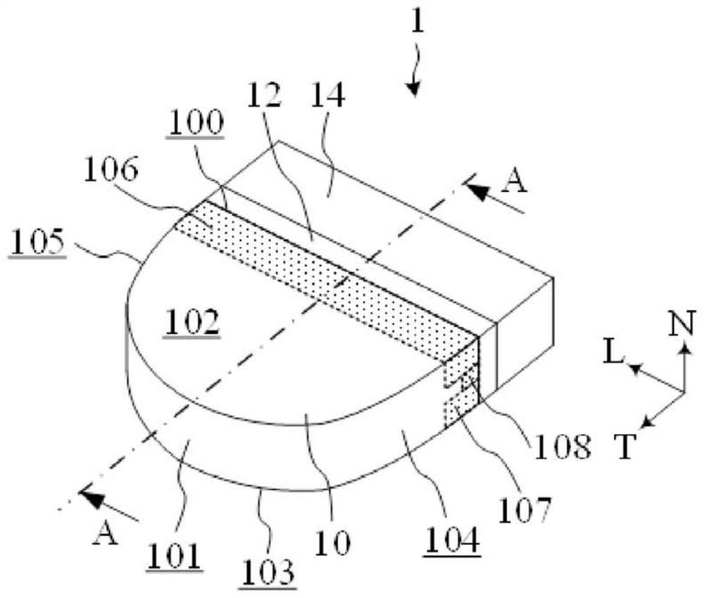
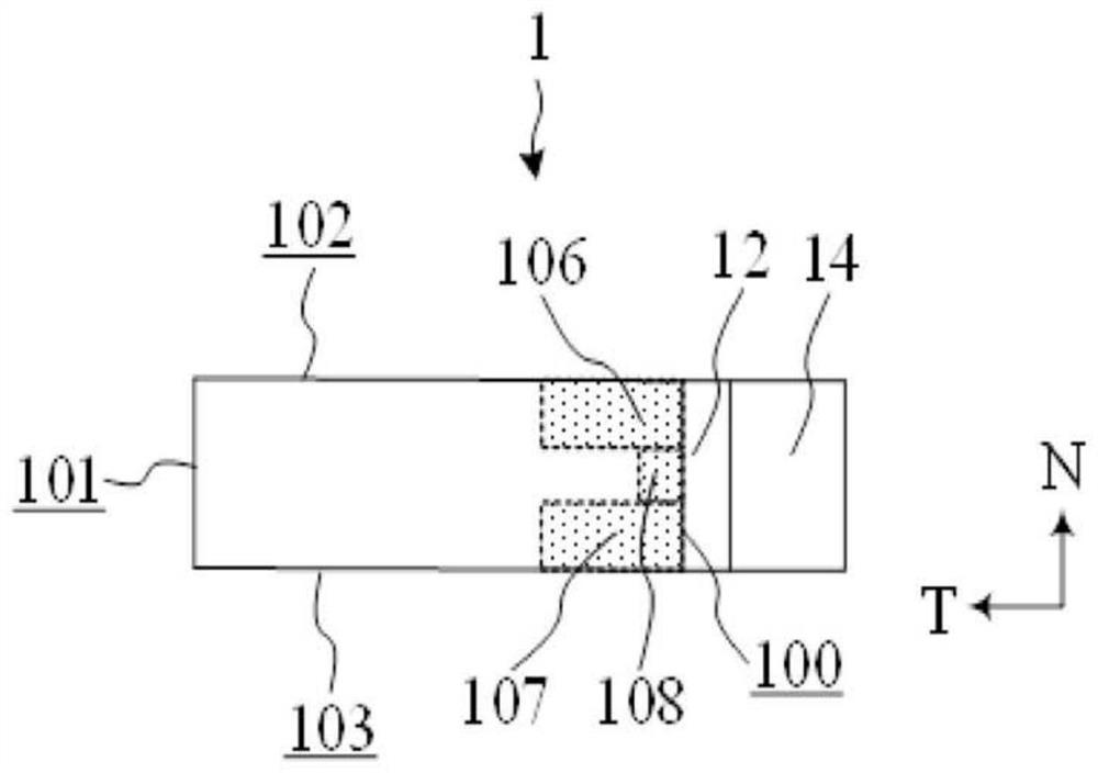
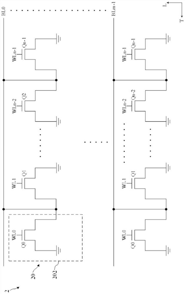
[0128] see image 3 , image 3 It is an equivalent circuit diagram of a NOR type memory element 2 according to a preferred embodiment of the present invention. In more detail, image 3 An equivalent circuit diagram of a NOR type memory element 2 with a vertical channel structure.

[0129] Such as image 3As shown, the memory cell array in the NOR memory device 2 according to the present invention includes a plurality of memory cell strings 20 along the lateral direction T. As shown in FIG. Each memory cell string 20 is composed of a plurality of memory cell blocks 202 connected in parallel to a corresponding bit line (BL0 to BLm−1) among the plurality of bit lines (BL0 to BLm−1). Each memory cell string 20 includes a corresponding bit line (BL0 to BLm−1) among the plurality of bit lines (BL0 to BLm−1) and a plurality of memory cells (Q0 to Qn−1). Each memory cell block 202 is composed of one memory cell (Q0 to Qn−1) among the plurality of memory cells (Q0 to Qn−1). Each ...


PUM


Abstract

The invention provides an NOR-type memory element. The NOR-type memory element comprises a plurality of bit lines formed on a semiconductor substrate, a plurality of first isolation strips, a plurality of second isolation strips, a plurality of memory units formed between the first isolation strips and the second isolation strips, a plurality of word lines and a grounding layer formed above the first isolation strips and the second isolation strips which are formed on a semiconductor substrate. The semiconductor substrate defines a longitudinal direction, a lateral direction, a plurality of columns along the longitudinal direction, and a plurality of rows in the lateral direction. The first isolation strips and the second isolation strips extend in the longitudinal direction. Each memory cell corresponds to one of the columns and one of the rows. The memory units located on one side of each first isolation strip and the memory units located on the other side of the first isolation strip are arranged in a staggered mode.

Description

technical field [0001] The present invention relates to a NOR type memory element and a method for manufacturing the NOR type memory element, in particular to a NOR type memory element comprising a plurality of vertical current mode sector field effect transistors (fan-shaped field effect transistor, FanFET) and A method of manufacturing the NOR type memory element. Background technique [0002] see figure 1 and figure 2 , these figures schematically depict the vertical current mode sector field effect transistor 1 disclosed by US Patent Publication No. 2019123060A1. figure 1 It is an external view of the vertical current mode sector field effect transistor 1 . figure 2 for figure 1 A cross-sectional view of a medium vertical current mode Sector Field Effect Transistor 1 along line A-A. [0003] Such as figure 1 and figure 2 As shown, the conventional vertical current mode sector field effect transistor 1 includes a pillar 10 formed of semiconductor material, a gat...

Claims


Application Information

Patent Timeline
Patent Type & Authority Applications(China)
IPC IPC(8): H01L27/11521H01L27/11568
CPCH10B43/30H10B41/30H01L29/40117H01L29/7926H10B43/10H10B43/27H01L29/66833H01L29/4234H01L23/528H01L23/5226H01L21/02532H01L21/76224H01L21/02595H01L21/32133H01L21/76877H01L21/76802H01L29/40114G11C11/4087H01L29/7827H10B12/03H10B12/05H10B12/30H10B12/31H10B12/48H10B12/315H10B41/10H10B41/27H10B12/37H10B12/038
Inventor 王振志何立玮
Owner 王振志
Why Eureka
Try Eureka