Electronic chip detection device

A detection device and electronic chip technology, applied in the direction of measuring devices, electronic circuit testing, measuring electricity, etc., can solve problems such as errors, detection probe shaking, and affecting detection accuracy, so as to reduce manpower, high detection efficiency, and accurate detection accuracy Effect

Inactive Publication Date: 2020-11-17
张克引
View PDF0 Cites 4 Cited by
  • Summary
  • Abstract
  • Description
  • Claims
  • Application Information

AI Technical Summary

Problems solved by technology

[0002] The chip generally refers to the carrier of the integrated circuit, which is also the result of the design, manufacture, packaging, and testing of the integrated circuit. It is usually an independent whole that can be used immediately. After the electronic chip equipment is produced, the electronic chip needs to be Comprehensive testing and testing of various currents and voltages. The current detection method for electronic chips is to detect workers holding detection probes drawn from the electrical testing box and observing the status of the indicator lights on the electrical testing box and the display screen. The size of the parameter is used to determine whether the electronic chip is qualified. During the detection process, the worker's hand-held detection probe is prone to shaking and causing errors, which affects the detection accuracy.

Method used


Image

  • Electronic chip detection device
  • Electronic chip detection device
  • Electronic chip detection device

Examples


specific Embodiment approach 1

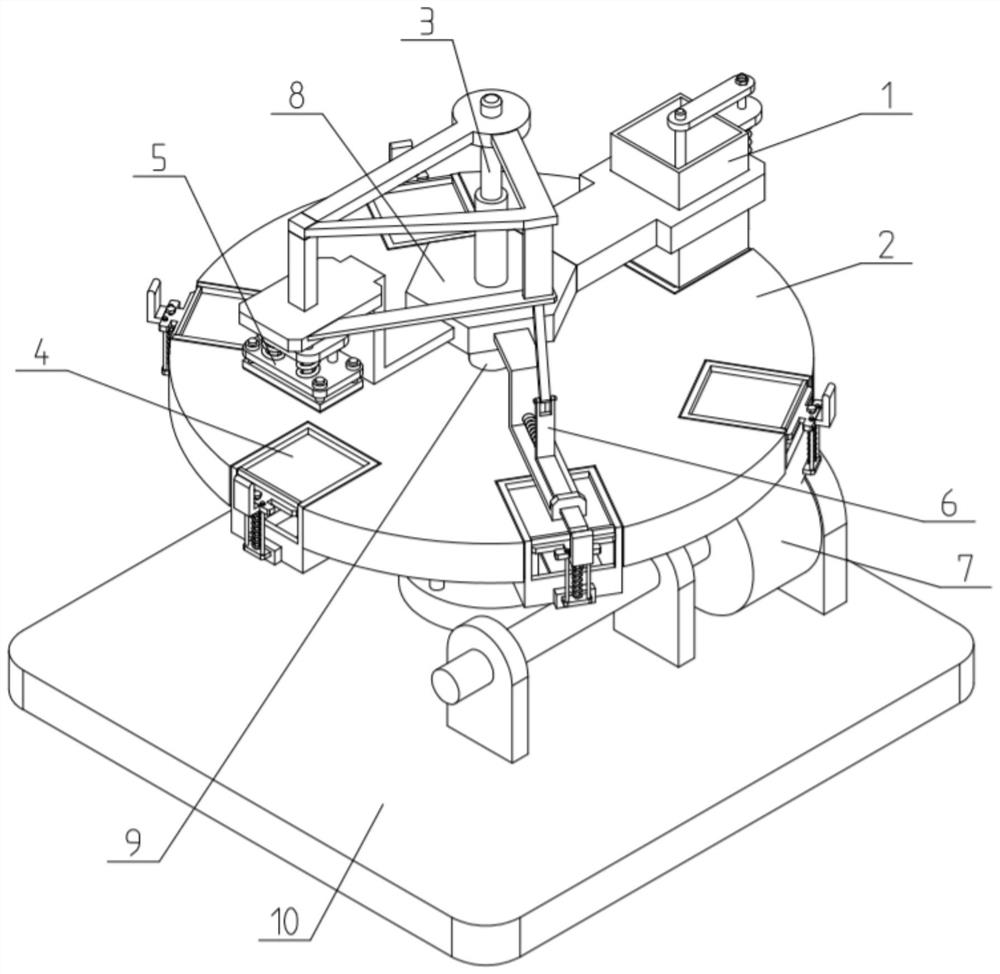
[0038] like Figure 1-11 As shown, the electronic chip detection device includes a chip storage mechanism 1, a rotating tray mechanism 2, a first driving mechanism 3, a detection and accommodating mechanism 4, a chip detection mechanism 5, a chip ejection mechanism 6, a second driving mechanism 7, a hexagonal seat The plate 8, the column 9 and the base 10, the upper and lower ends of the column 9 are respectively fixedly connected with the center of the hexagonal seat plate 8 and the center of the base 10; The middle of the column 9; the second driving mechanism 7 is fixedly connected to the base 10; the second driving mechanism 7 is drivingly connected to the rotating tray mechanism 2; the rotating tray mechanism 2 is evenly arranged around Six detection and accommodating mechanisms 4;

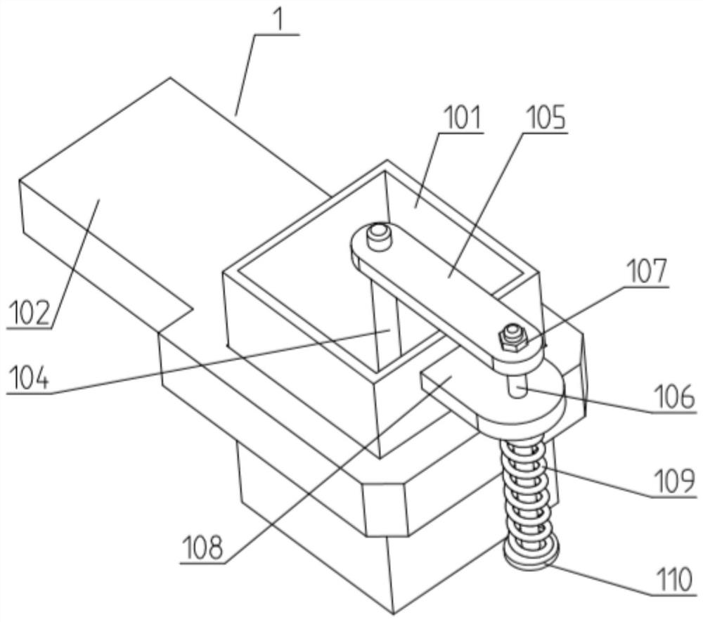
[0039] The chip storage mechanism 1 , the chip detection mechanism 5 and the chip push-out mechanism 6 are fixedly connected on the three sides of the hexagonal base plate 8 ; the chip stora...

specific Embodiment approach 2

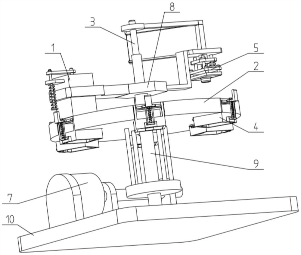
[0041] like Figure 1-11 As shown, the rotating tray mechanism 2 includes a circular turntable 201, a linkage column 202 and a worm gear 203; the bottom surface of the circular turntable 201 is fixedly connected to the top surface of the worm gear 203 through a plurality of linkage columns 202 evenly arranged around it; The circular turntable 201 and the worm gear 203 are respectively rotatably fitted on the upper and lower ends of the upright column 9 by means of seated bearings; six detection and accommodating mechanisms 4 are evenly arranged around the circular turntable 201 ; the second The drive mechanism 7 is drivingly connected to the worm gear 203 .

[0042] The second drive mechanism 7 includes a servo motor 701, a worm 702 and a rod seat 703; the servo motor 701 is fixedly connected to the base 10 through a motor bracket; the output shaft of the servo motor 701 is connected through a coupling The worm 702; the worm 702 is rotatably connected to the two rod bases 703...

specific Embodiment approach 3

[0045] like Figure 1-11 As shown, the detection and accommodating mechanism 4 includes a accommodating box 401 , an attachment plate 402 , an accommodating support plate 403 , a lifting slide plate 404 , an adjusting screw 405 , a limit slide plate 406 , an L-shaped linkage block 407 , and a horizontal sliding frame 408 , reset tension spring 409 and tension spring seat plate 410; the top and bottom surfaces of the accommodating box 401 are both open; the top surface of the accommodating box 401 is coplanar with the top surface of the circular turntable 201; The accommodating box 401 is matched and connected in the opening groove of the circular turntable 201; the inner end of the accommodating box 401 is fixedly connected with an adapter plate 402, and the adapter plate 402 is fixedly connected to the On the bottom surface of the circular turntable 201; two longitudinal slideways are provided on both sides of the outer end of the accommodating box 401, and the two ends of th...


PUM


Abstract

The invention relates to the technical field of chip detection, in particular to an electronic chip detection device, which comprises a chip storage mechanism, a rotary tray mechanism, a first drivingmechanism, a detection accommodating mechanism, a chip detection mechanism, a chip push-out mechanism, a second driving mechanism, a hexagonal seat plate, an upright post and a base, the upper end and the lower end of the upright post are fixedly connected with the center of the hexagonal base plate and the center of the base respectively. The rotary tray mechanism is connected to the middle of the upright post in a running fit mode. The second driving mechanism is fixedly connected to the base; the second driving mechanism is in transmission connection with the rotary tray mechanism; six detection accommodating mechanisms are uniformly arranged on the rotary tray mechanism in a surrounding manner; according to the invention, the placement of the electronic chip, the detection of the electronic chip and the ejection work of the electronic chip after detection can be achieved, the detection precision of the electronic chip is more accurate, and the detection efficiency is higher.

Description

technical field [0001] The present invention relates to the technical field of chip detection, and more particularly, to an electronic chip detection device. Background technique [0002] The chip generally refers to the carrier of the integrated circuit, and it is also the result of the design, manufacture, packaging and testing of the integrated circuit. It is usually an independent whole that can be used immediately. After the electronic chip equipment has produced the electronic chip, the electronic chip needs to be processed. Comprehensive testing and testing of various currents and voltages, the current detection method of electronic chips is to detect workers holding detection probes drawn from the electrical testing box, and observing the status of the indicator lights on the electrical testing box and the display on the display. The size of the parameters determines whether the electronic chip is qualified or not. During the detection process, the worker's hand-held...

Claims


Application Information

Patent Timeline
Patent Type & Authority Applications(China)
IPC IPC(8): G01R31/28
CPCG01R31/2886G01R31/2893
Inventor 张克引
Owner 张克引
Why Eureka
Try Eureka