
Trench gate mosfet device and manufacturing method thereof

A device manufacturing method and slot grid technology, which are applied in semiconductor/solid-state device manufacturing, semiconductor devices, electric solid-state devices, etc., can solve problems affecting the normal operation of devices, improve the ability to resist single-event burnout, reduce resistance, reduce area effect

Active Publication Date: 2021-01-12
BEIJING ZHONGKE XINWEITE SCI & TECH DEV
View PDF3 Cites 0 Cited by
  • Summary
  • Abstract
  • Description
  • Claims
  • Application Information

AI Technical Summary

Problems solved by technology

[0005] When the trench gate MOSFET device is in the blocking state, the current pulse generated by the high-energy particle radiation triggers the parasitic triode, which causes a single event effect and affects the normal operation of the device.

Method used


Image

  • Trench gate mosfet device and manufacturing method thereof
  • Trench gate mosfet device and manufacturing method thereof
  • Trench gate mosfet device and manufacturing method thereof

Examples


Embodiment Construction

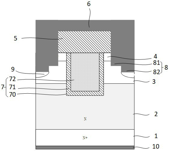
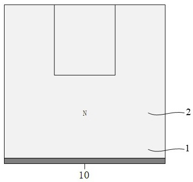
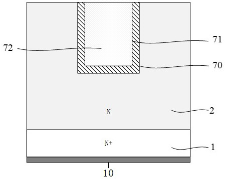
[0038] Features and exemplary embodiments of various aspects of the invention will be described in detail below. In the following detailed description, numerous specific details are set forth in order to provide a thorough understanding of the present invention. It will be apparent, however, to one skilled in the art that the present invention may be practiced without some of these specific details. The following description of the embodiment is only to provide a better understanding of the present invention by showing examples of the present invention, the present invention is by no means limited to any specific configuration and algorithm proposed below, but without departing from the scope of the present invention Any modifications, substitutions, and improvements of elements, components, and algorithms are covered within the spirit of the present invention. In the drawings and the following description, well-known structures and techniques are not shown in order to avoid u...


PUM


Abstract

The present application provides a trench gate MOSFET device and a manufacturing method thereof, belonging to the technical field of semiconductors. The trench gate MOSFET device comprises: a substrate, an epitaxial layer, a well region, a source region, an interlayer dielectric layer and a first layer stacked in sequence. an electrode layer; and a trench gate, including a gate trench, a gate dielectric layer and a gate conductive material layer, a part of the gate trench is located in the epitaxial layer, a part is located in the well region, and the gate dielectric layer is located at the bottom of the gate trench On the surface and side, the gate conductive material layer is filled in the gate trench; the source contact hole is formed by extending the interlayer dielectric layer to the well region, and the first electrode layer is connected to the source region and the well region through the source contact hole, and the source contact hole It includes a first contact hole and a second contact hole that communicate with each other, the diameter of the first contact hole is larger than that of the second contact hole, and the first contact hole is distributed close to the first electrode layer. The present application improves the device's resistance to single event burnout.

Description

technical field [0001] The application belongs to the technical field of semiconductors, and relates to a trench gate MOSFET device and a manufacturing method thereof. Background technique [0002] In the field of semiconductor technology, Metal-Oxide-Semiconductor Field-Effect Transistor (MOSFET) is a field-effect transistor (field-effect transistor) that can be widely used in analog circuits and digital circuits. , The trench gate MOSFET can achieve low resistance and high current due to its small cell size. When applied in a specific environment, continuous high-energy particle radiation can easily induce single event effects in MOSFETs, resulting in catastrophic accidents in the application system. Therefore, it is necessary to provide a trench-gate MOSFET device to improve the anti-single event capability of the device . [0003] A trench-gate MOSFET device provided by the related art includes a gate layer for controlling switching of a transistor; a drain and a sourc...

Claims


Application Information

Patent Timeline
Patent Type & Authority Patents(China)
IPC IPC(8): H01L29/78H01L23/552H01L21/336
CPCH01L23/552H01L29/66734H01L29/7803H01L29/7813
Inventor 龚雪芹张彦飞郝乐刘梦新
Owner BEIJING ZHONGKE XINWEITE SCI & TECH DEV
Features
  • Generate Ideas
  • Intellectual Property
  • Life Sciences
  • Materials
  • Tech Scout
  • Unparalleled Data Quality
  • Higher Quality Content
  • 60% Fewer Hallucinations
Learn More