
Display panel and display device

A technology of display panel and display area, applied in the direction of diodes, semiconductor devices, electrical components, etc., can solve the problems of electronic equipment not being a full screen, bad dark spots, unable to display, etc.

Active Publication Date: 2020-12-04
KUNSHAN GO VISIONOX OPTO ELECTRONICS CO LTD
View PDF3 Cites 1 Cited by
  • Summary
  • Abstract
  • Description
  • Claims
  • Application Information

AI Technical Summary

Problems solved by technology

Traditional electronic devices such as mobile phones, tablet computers, etc., need to integrate such as front camera, earpiece, and infrared sensing components, so it is possible to set the camera, earpiece, and infrared sensing elements in the slotted area by slotting (Notch) on the display screen. Components, etc., but these electronic devices are not truly full-screen, and cannot be displayed in all areas of the entire screen, such as the image cannot be displayed in the camera area
[0003] In order to achieve a true full screen, the camera technology under the screen came into being, that is, the area of ​​the display screen where the photosensitive device is set can still be used for display, but there will be dark spots in this area during normal display.

Method used


Image

  • Display panel and display device
  • Display panel and display device

Examples


Embodiment Construction

[0023] In order to facilitate the understanding of the present invention, the present invention will be described more fully below with reference to the associated drawings. The present invention can be implemented in many different forms and is not limited to the embodiments described herein.

[0024] One or more embodiments of the present invention will be described in detail with reference to the accompanying drawings, and elements such as shapes, dimensions, proportions, angles, and quantities of elements in the drawings are merely examples, and in different embodiments, the same or corresponding elements can be The same reference numerals are shown, and repeated explanations are omitted.

[0025] Unless otherwise defined, all technical and scientific terms used herein have the same meaning as commonly understood by one of ordinary skill in the technical field of the invention. As used herein, the term "and / or" includes any and all combinations of one or more of the assoc...


PUM


Abstract

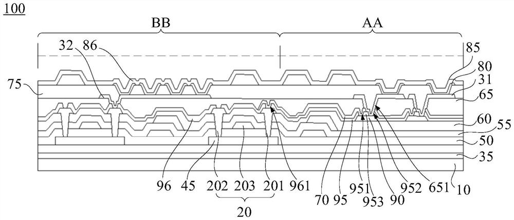
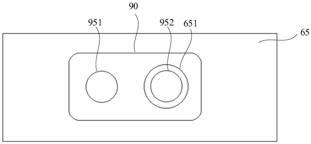
The invention relates to a display panel and a display device. The display panel is provided with a first display area and a second display area, the light transmittance of the first display area is higher than that of the second display area, the display panel comprises a substrate, a driving layer set and an anode layer which are arranged in a stacked mode, the driving layer set is located in the second display area, and the anode layer comprises a first anode located in the first display area. The first anode is electrically connected with a drain electrode of the driving layer group through a wire; the display panel further comprises a first isolation layer and a lap joint layer which are located in the first display area, the first isolation layer is arranged between the lap joint layer and the wires and provided with first via holes, and the wires pass through the first via holes and are connected with the lap joint layer so as to enable the first anode to be electrically connected with the drain electrode of the driving layer set. According to the display panel and the display device provided by the invention, low-resistance lap joint is formed between the wiring and the lapjoint layer through the first via hole, so that influence of lap joint impedance on the potential between the first anode and the wiring is reduced, and virtual dark spots in the first display area are avoided.

Description

technical field [0001] The present invention relates to the field of display technology, in particular to a display panel and a display device. Background technique [0002] With the rapid development of electronic devices, users have higher and higher requirements for screen-to-body ratio, so that the full-screen display of electronic devices has attracted more and more attention from the industry. Traditional electronic devices such as mobile phones, tablet computers, etc., need to integrate such as front camera, earpiece, and infrared sensing components, so it is possible to set the camera, earpiece, and infrared sensing elements in the slotted area by slotting (Notch) on the display screen. Components, etc., but these electronic devices are not truly full-screen, and cannot be displayed in all areas of the entire screen, for example, images cannot be displayed in the camera area. [0003] In order to achieve a true full screen, the under-screen camera technology has eme...

Claims


Application Information

Patent Timeline
IPC IPC(8): H01L27/32
CPCH10K59/65H10K59/12H10K59/131H10K59/1213H10K2102/302H10K59/122H10K2102/101H10K59/8051H10K59/60
Inventor 金玉王恩来陆蕴雷李磊张鹏辉马明冬
Owner KUNSHAN GO VISIONOX OPTO ELECTRONICS CO LTD
Learn More