Lead frame plate placing and pushing-out equipment for semiconductor cutting

A lead frame and semiconductor technology, applied in semiconductor/solid-state device manufacturing, semiconductor devices, semiconductor/solid-state device components, etc., can solve the problems of increasing the work intensity of operators and reducing the efficiency of semiconductor tailoring, so as to improve the tailoring Efficiency, the effect of avoiding manual picking and placing

Inactive Publication Date: 2020-12-15
李锋
View PDF0 Cites 2 Cited by
  • Summary
  • Abstract
  • Description
  • Claims
  • Application Information

AI Technical Summary

Problems solved by technology

[0002] As the chip carrier of the inherited circuit, the lead frame acts as a bridge connecting the external wires. Most of the semiconductor integrated blocks need to use the lead frame. It is an important basic material in the electronic information industry. In order to improve production efficiency and improve material The utilization rate of semiconductors is convenient for batch processing of semiconductors. Therefore, a common lead frame is equipped with multiple chip nodes, and multiple chips are set on the chip nodes. After curing and packaging, the production of semiconductors is completed. After the production is completed , the semiconductor needs to be cut off from the lead frame, and the existing tailoring uses mechanical equipment for semiconductor tailoring, and the lead frames are placed in the tailoring device one by one continuously before cutting, although this method can realize However, since the lead frames need to be placed in the cutting device one by one by a special person, the work intensity of the operator is firstly increased, and the operator needs to place the lead frames continuously when the cutting device is running, which reduces the cutting of semiconductors. system efficiency

Method used


Image

  • Lead frame plate placing and pushing-out equipment for semiconductor cutting
  • Lead frame plate placing and pushing-out equipment for semiconductor cutting
  • Lead frame plate placing and pushing-out equipment for semiconductor cutting

Examples


Embodiment 1

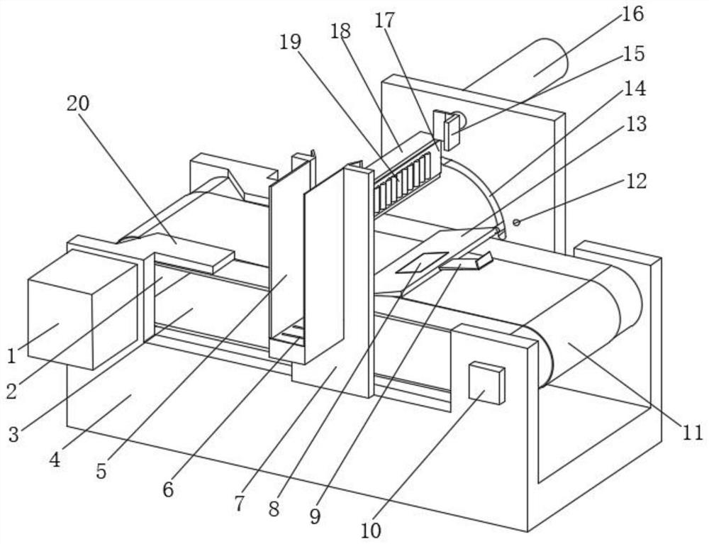
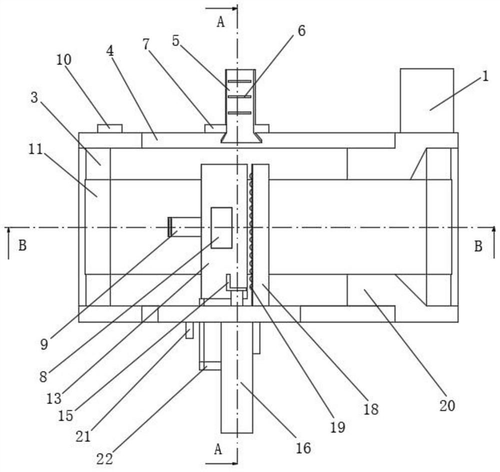
[0028] Embodiment 1: A semiconductor tailoring lead frame plate placing and pushing out device includes a base 4, a top frame 18 and a second motor 23;

[0029] Base 4: its back side is provided with arc hole 14, and its back side is provided with detection hole 12, and detection hole 12 is positioned at the right side of the lower end of arc hole 14, and the back side of base 4 is fixed with sensor 21, and sensor 21 and detection The holes 12 are arranged in front and back correspondingly. There are two transmission rollers 2 rotating inside the base 4, and the two transmission rollers 2 are connected by a belt 3. The front side of the base 4 is fixed with a first motor 1, and the output end of the first motor 1 passes through the The front side of the base 4 is fixed on the front end of one of the driving rollers 2, the rear side of the base 4 is fixed with an electric push rod 16, and the output end of the electric push rod 16 passes through the rear side of the base 4 and i...

Embodiment 2

[0034] The difference between this embodiment and Embodiment 1 is:

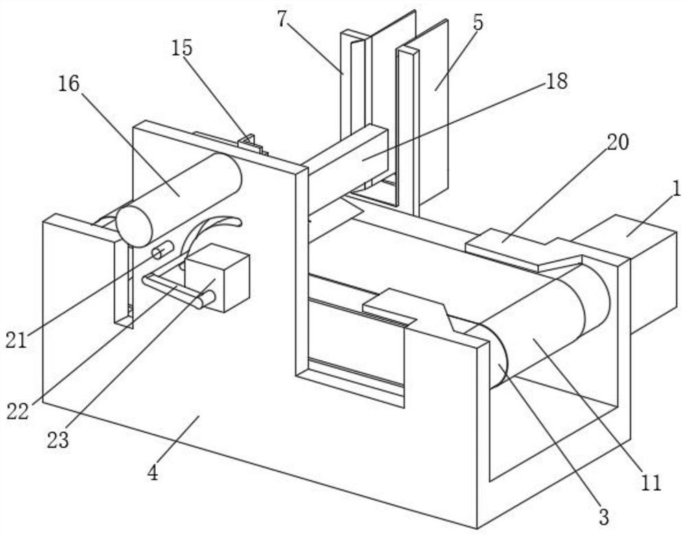
[0035] In this embodiment, it also includes a discharge frame 5 and a support plate 7, the lower end of the support plate 7 is fixed on the upper side of the front end of the base 4, the discharge frame 5 passes through the support plate 7, and the discharge frame 5 and the push seat 15 front and back Corresponding to the setting, the lead frame board can be pushed into the designated equipment through the discharge frame 5, and the first built-in roller 6 is also included, which is rotated in the inner lower side of the discharge frame 5 through the rotating shaft, and its linear array is arranged on the In the inner lower side of the discharge frame 5, its upper half side is located above the inner lower side of the discharge frame 5, and the friction between the lower end of the lead frame plate and the discharge frame 5 is reduced by the first embedded roller 6, and the friction between the lower end of th...

Embodiment 3

[0037] The difference between this embodiment and embodiment two is:

[0038] In this embodiment, a magnet 8 is also included, which is interspersed in the upper side of the turnover plate 13, and the lead frame plate is attracted by the magnet 8, so as to prevent the lead frame plate from slipping when the turnover plate 13 is turned over, and a baffle plate 9 is also included, which is fixed on The right end of turnover plate 13, prevents lead frame plate from rushing out of turnover plate 13 to the right by baffle plate 9, also includes increasing friction strip 11, is fixed on the outer surface of belt 3, prevents lead frame plate from being on belt 3 by increasing friction strip 11 Glide on.

[0039] When in use: the lead frame plate is sent to the friction-increasing strip 11 from the external production equipment, the single-chip microcomputer 10 is turned on, the first motor 1 starts to work, the first motor 1 drives the driving roller 2 to rotate, and the driving roll...


PUM


Abstract

The invention discloses lead frame plate placing and pushing-out equipment for semiconductor cutting. The lead frame plate placing and pushing-out equipment comprises a base, a top frame and a secondmotor. An arc-shaped hole is formed in the rear side of the base, a detection hole is formed in the rear side of the base, the detection hole is located in the right of the lower end of the arc-shapedhole, a sensor is fixed to the rear side of the base, the sensor and the detection hole are arranged in a front-back corresponding mode, and two transmission rollers are rotationally arranged in thebase and are in transmission connection through a belt. A first motor is fixed to the front side of the base, the output end of the first motor penetrates through the front side of the base to be fixed to the front end of one of the transmission rollers, and an electric push rod is fixed to the rear side of the base. According to the lead frame plate placing and pushing-out equipment for semiconductor cutting, the lead frame plates can be placed into the equipment without stop, then the lead frame plates are turned over to be placed and pushed into the cutting device, manual taking and placingare avoided, and the cutting efficiency is improved.

Description

technical field [0001] The invention relates to the technical field of lead frame production equipment, in particular to a lead frame plate placement and ejection device for semiconductor tailoring. Background technique [0002] As the chip carrier of the inherited circuit, the lead frame acts as a bridge connecting the external wires. Most of the semiconductor integrated blocks need to use the lead frame. It is an important basic material in the electronic information industry. In order to improve production efficiency and improve material The utilization rate of semiconductors is convenient for batch processing of semiconductors. Therefore, a common lead frame is equipped with multiple chip nodes, and multiple chips are set on the chip nodes. After curing and packaging, the production of semiconductors is completed. After the production is completed , the semiconductor needs to be cut off from the lead frame, and the existing tailoring uses mechanical equipment for semicon...

Claims


Application Information

Patent Timeline
IPC IPC(8): H01L21/677H01L23/495
CPCH01L21/67721H01L23/495
Inventor 李锋
Owner 李锋
Why Eureka
Try Eureka