Ferroelectric domain defined series two-dimensional photovoltaic cell and preparation method thereof
A photovoltaic cell and ferroelectric domain technology, applied in the field of two-dimensional semiconductor photovoltaic devices, can solve the problems of complicated process and difficult control of doping level, and achieve the effect of avoiding polluting materials and reducing energy consumption
- Summary
- Abstract
- Description
- Claims
- Application Information
AI Technical Summary
Problems solved by technology
Method used
Image
Examples
Embodiment example 1
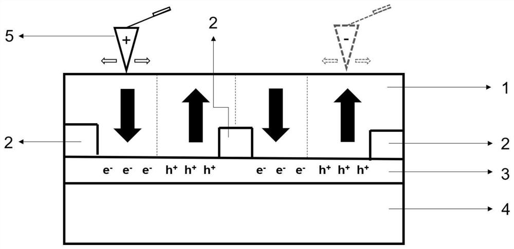
[0037] The specific steps for implementing Case 1 are as follows:
[0038] 1) Insulator silicon substrate preparation
[0039] The silicon-insulator substrate is a silicon substrate whose surface is covered with silicon dioxide with a thickness of 285 nm.
[0040] 2) Preparation and transfer of two-dimensional semiconductors of bipolar transition metal compounds
[0041] 8-nm ambipolar transition metal compound two-dimensional semiconductor MoTe by mechanical exfoliation 2 onto a silicon-insulator substrate.
[0042] 3) Metal electrode preparation
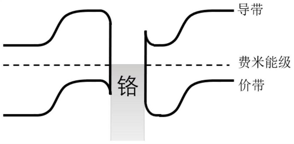
[0043] The metal electrode 3 is prepared by using ultraviolet lithography or electron beam exposure technology combined with thermal evaporation and lift-off process. The electrodes consist of chromium and gold with a thickness of 15 nanometers for chromium and 25 nanometers for gold. The prepared three metal electrodes are respectively located at both ends and in the middle of the bipolar transition metal compound two-dimensi...
Embodiment example 2
[0048] The specific steps for implementing Case 2 are as follows:
[0049] 1) Insulator silicon substrate preparation
[0050] The silicon-insulator substrate is a silicon substrate whose surface is covered with silicon dioxide with a thickness of 285 nm.
[0051] 2) Preparation and transfer of two-dimensional semiconductors of bipolar transition metal compounds
[0052] 10-nanometer bipolar transition metal compound two-dimensional semiconductor MoTe by mechanical exfoliation 2 onto a silicon-insulator substrate.
[0053] 3) Metal electrode preparation
[0054] The metal electrode 3 is prepared by using ultraviolet lithography or electron beam exposure technology combined with thermal evaporation and lift-off process. The electrodes consist of chromium and gold with a thickness of 15 nanometers for chromium and 25 nanometers for gold. The prepared three metal electrodes are respectively located at both ends and in the middle of the bipolar transition metal compound two-d...
Embodiment example 3
[0059] The specific steps for implementing Case 3 are as follows:
[0060] 1) Insulator silicon substrate preparation
[0061] The silicon-insulator substrate is a silicon substrate whose surface is covered with silicon dioxide with a thickness of 285 nm.
[0062] 2) Preparation and transfer of two-dimensional semiconductors of bipolar transition metal compounds
[0063] 12-nanometer bipolar transition metal compound two-dimensional semiconductor MoTe by mechanical exfoliation 2 onto a silicon-insulator substrate.
[0064] 3) Metal electrode preparation
[0065] The metal electrode 3 is prepared by using ultraviolet lithography or electron beam exposure technology combined with thermal evaporation and lift-off process. The electrodes consist of chromium and gold with a thickness of 15 nanometers for chromium and 25 nanometers for gold. The prepared three metal electrodes are respectively located at both ends and in the middle of the bipolar transition metal compound two-d...
PUM
| Property | Measurement | Unit |
|---|---|---|
| thickness | aaaaa | aaaaa |
| thickness | aaaaa | aaaaa |
| thickness | aaaaa | aaaaa |
Abstract
Description
Claims
Application Information
 - R&D
- Intellectual Property
- Life Sciences
- Materials
- Tech Scout
- Unparalleled Data Quality
- Higher Quality Content
- 60% Fewer Hallucinations
Browse by: Latest US Patents, China's latest patents, Technical Efficacy Thesaurus, Application Domain, Technology Topic, Popular Technical Reports.
© 2025 PatSnap. All rights reserved.Legal|Privacy policy|Modern Slavery Act Transparency Statement|Sitemap|About US| Contact US: help@patsnap.com


