Display panel, manufacturing method thereof and display device
A technology for display panels and substrates, which is used in semiconductor/solid-state device manufacturing, organic semiconductor devices, electrical components, etc., and can solve problems such as poor display effect of OLED display panels
- Summary
- Abstract
- Description
- Claims
- Application Information
AI Technical Summary
Problems solved by technology
Method used
Image
Examples
Embodiment Construction
[0055] In order to make the purpose, technical solution and advantages of the present application clearer, the implementation manners of the present application will be further described in detail below in conjunction with the accompanying drawings.
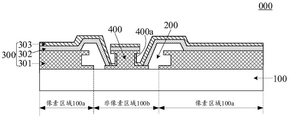
[0056] Please refer to figure 1 , figure 1 It is a schematic diagram of the film layer structure of a display panel provided in the embodiment of the present application. The display panel 000 may include:
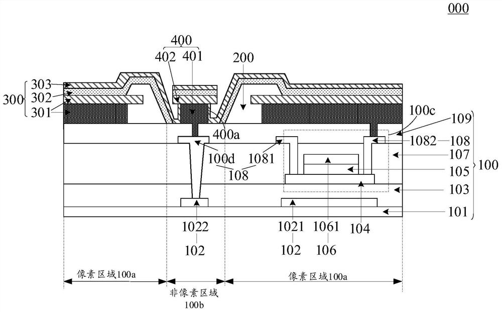
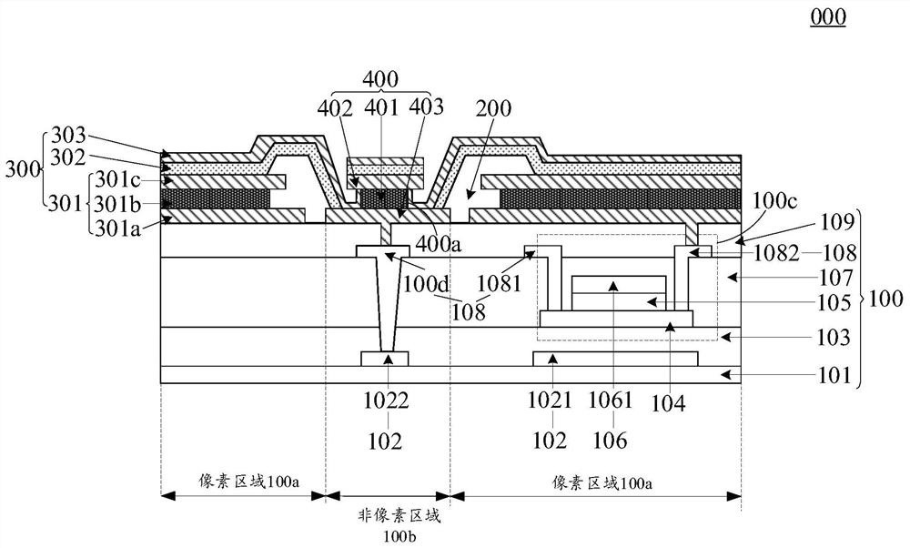
[0057] The substrate 100 , and the pixel defining layer 200 , the light emitting device 300 and the auxiliary electrode layer 400 located on the substrate 100 .
[0058] The pixel defining layer 200 on the substrate 100 is used to define on the substrate 100: a plurality of pixel regions 100a, and a non-pixel region 100b located around the pixel regions 100a.
[0059] The light emitting device 300 on the substrate 100 may be located in the pixel region 100a. It should be noted that the number of light-emitting devices 300...
PUM
 Abstract
Description
Claims
Application Information


