Rapid optimization method for optical reverse design
An optimization method and reverse design technology, applied in the field of integrated optics, can solve the problems of consuming computing resources, multiplying time and computing resources, and consuming a lot of time, and achieve the effect of saving computing resources, shortening optimization time, and reducing time.
Active Publication Date: 2021-01-05
LANZHOU UNIVERSITY
View PDF7 Cites 5 Cited by
- Summary
- Abstract
- Description
- Claims
- Application Information
AI Technical Summary
Problems solved by technology
However, the traversal search consumes a huge amount of computing resources. In the case of limited computing resources, using the reverse design method of DBS will consume a lot of time
And as the area of the solution space increases, the time and computing resources consumed by the DBS optimization method are doubling.
Another commonly used optimization me
Method used
View moreImage
Smart ImageViewing Examples

Examples
 PUM
 Abstract
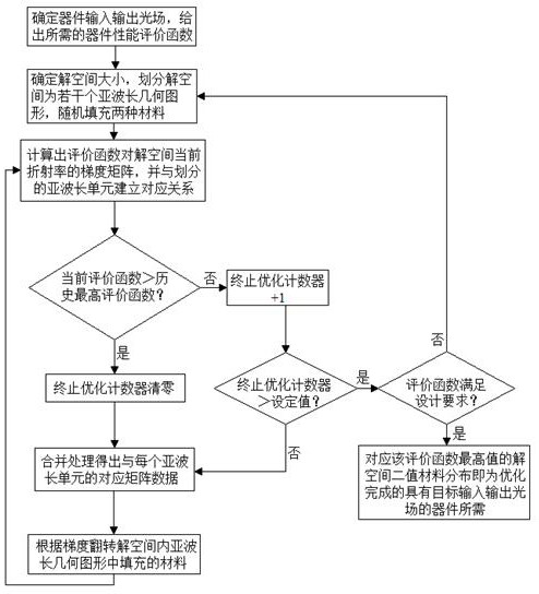
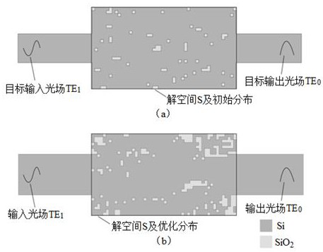
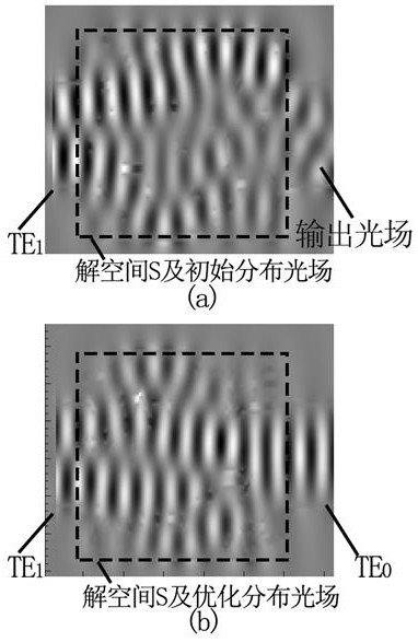
The invention discloses a rapid optimization method for optical reverse design. The method comprises the following steps: determining the sizes and shapes of an input and output light field and a solution space of a device according to an optimization target; dividing the solution space into a plurality of sub-wavelength units which are respectively occupied by a waveguide layer material and a cladding layer material of the device; calculating the gradient of the evaluation function for the refractive index of the corresponding position in the solution space; and according to the gradient, establishing a corresponding relationship with each sub-wavelength unit in the solution space through a merging method, adjusting the binarized material filled in the sub-wavelength units in the solutionspace, and obtaining the final solution space material distribution through multiple iterative processes. The material distribution of the solution space is adjusted by adopting a binary search mode,and the material occupied in the sub-wavelength unit is guided to turn over by calculating the gradient of the refractive index of the evaluation function to the corresponding position in the solution space. Compared with a direct binarization search algorithm, the method of the invention has the advantages that the optimization time can be greatly shortened, and computing resources are saved.
Description
technical field [0001] The invention belongs to the technical field of integrated optics, and relates to a fast optimization method for optical reverse design. Background technique [0002] In recent years, with the advent of the era of big data and the rapid rise of applications requiring massive data processing, the requirements for data interconnection, processing capacity and speed are getting higher and higher. Compared with the traditional electrical interconnection field, the optical signal has the characteristics of high speed, high frequency, large bandwidth, strong anti-interference ability, etc. Therefore, the use of optical signal transmission and data processing has higher speed and larger capacity. One of the main functions of optical device design is to control the light field. [0003] Optical inverse design is a design method for effectively manipulating the light field in an ultra-compact space. It can make full use of the degree of freedom of spatial var...
Claims
Login to View More Application Information
Patent Timeline
 IPC IPC(8): G02B27/00
CPCG02B27/0012
Inventor 贾浩陈豪翔杨建红王涛
Owner LANZHOU UNIVERSITY
Features
- R&D
- Intellectual Property
- Life Sciences
- Materials
- Tech Scout
- Unparalleled Data Quality
- Higher Quality Content
- 60% Fewer Hallucinations
Learn More Browse by: Latest US Patents, China's latest patents, Technical Efficacy Thesaurus, Application Domain, Technology Topic, Popular Technical Reports.
© 2025 PatSnap. All rights reserved.Legal|Privacy policy|Modern Slavery Act Transparency Statement|Sitemap|About US| Contact US: help@patsnap.com