
A rapid crimp detection device for optical chips

A detection device and optical chip technology, applied in the direction of measuring devices, instruments, etc., can solve the problems of increasing the test process, affecting the heat conduction of the chip carrier, and the connection between the chip carrier and the heat sink block is not tight, so as to achieve chip temperature control, Avoid uneven heat dissipation and realize the effect of standardized detection

Active Publication Date: 2021-03-02
上海菲莱测试技术有限公司
View PDF8 Cites 0 Cited by
  • Summary
  • Abstract
  • Description
  • Claims
  • Application Information

AI Technical Summary

Problems solved by technology

[0003] 1. Due to the flatness problem of the chip carrier itself and the flatness problem caused by the cooperation between the chip carrier and the heat sink block, it is easy to have poor chip contact between the chip carrier and the pin block caused by insufficient pressure. It is easy to cause the chip carrier and the heat sink to be not tightly connected, thereby affecting the heat conduction at different positions of the chip carrier and affecting the thermal uniformity of the chip;
[0004] 2. The operator needs to manually control the pressure needle block to form a circuit, which requires high personal operation, errors are prone to occur, standardized detection cannot be realized, and the labor cost is high and the operation time is long;
[0005] 3. The aging detection and optical power detection need to be carried out twice, and the chip needs to be re-placed and pressed twice, which increases the test process, affects the test efficiency, and increases the operating cost

Method used


Image

  • A rapid crimp detection device for optical chips
  • A rapid crimp detection device for optical chips
  • A rapid crimp detection device for optical chips

Examples


Embodiment Construction

[0079] Embodiments of the technical solutions of the present invention will be described in detail below in conjunction with the accompanying drawings. The following examples are only used to illustrate the technical solutions of the present invention more clearly, and therefore are only examples, rather than limiting the protection scope of the present invention.

[0080] It should be noted that, unless otherwise specified, the technical terms or scientific terms used in this application shall have the usual meanings understood by those skilled in the art to which the present invention belongs.

[0081] In the description of this application, it is to be understood that the terms "central", "longitudinal", "transverse", "length", "width", "thickness", "vertical", "horizontal", "top", The orientation or positional relationship indicated by "bottom", "inner", "outer", etc. is based on the orientation or positional relationship shown in the drawings, and is only for the convenie...


PUM


Abstract

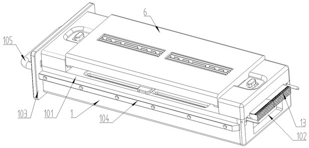
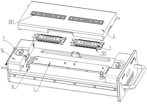
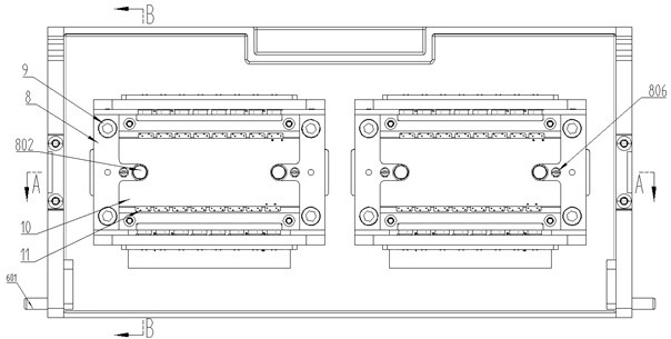
The invention discloses a quick pressure-bonding detection device for an optical chip, which comprises a lower casing fixed with a lower PCB board; a chip carrier mounted on the top surface of the lower casing and evenly placing chips; a chip temperature control mechanism arranged in the lower casing and the lower PCB board Electrical connection; the upper cover is located above the lower shell and one end is hinged with the lower shell, and a locking mechanism is arranged between the upper cover and the lower shell; the floating positioning plate is installed on the bottom surface of the upper cover, the upper PCB board is fixed on the bottom surface, and the bottom surface is installed with a spring The probe; the optical power detection mechanism is installed on the bottom surface of the upper PCB board; the connector is arranged on one side of the lower casing to be electrically connected to the lower PCB board. When the upper cover of the present invention is closed, the chip is powered on, and the optical power detection mechanism detects the optical power of the chip at the same time, which improves the test efficiency and reduces the cost; the floating positioning plate is floatingly installed to adapt to different chips, and the spring probe is used to effectively ensure that the chip is pressed tightly , to avoid poor contact and uneven heat dissipation; only need to control the upper cover to realize the pressing and electrification of the chip, which helps to achieve standardized testing.

Description

technical field [0001] The invention relates to the technical field of chip detection, in particular to a rapid crimping detection device for an optical chip. Background technique [0002] After the optical chip is manufactured, strict aging tests and optical power tests are required. During the test, it is necessary to ensure that the chip connection is stable, and adjust and maintain the test temperature, so as to determine the working state of the chip at different working temperatures. Existing chip testing devices generally place the chip on the chip carrier, place the chip carrier on the heat sink block used to control the temperature, manually press the needle block on the chip carrier to form a path, and then perform aging test and optical power test. The existing chip testing device has the following problems in the working process: [0003] 1. Due to the flatness problem of the chip carrier itself and the flatness problem caused by the cooperation between the ch...

Claims


Application Information

Patent Timeline
Patent Type & Authority Patents(China)
IPC IPC(8): G01D21/02
CPCG01D21/02
Inventor 张华薛银飞黄河
Owner 上海菲莱测试技术有限公司
Learn More