Layered electromagnetic shielding packaging structure and packaging structure manufacturing method

A packaging structure and electromagnetic shielding technology, applied in circuits, electrical components, electrical solid devices, etc., can solve problems such as difficulty in meeting the individual shielding requirements of electronic products and cumbersome packaging processes.

Active Publication Date: 2021-02-26
FOREHOPE ELECTRONICS NINGBO CO LTD
View PDF5 Cites 0 Cited by
  • Summary
  • Abstract
  • Description
  • Claims
  • Application Information

AI Technical Summary

Problems solved by technology

The packaging process in this way is cumbersome, and the shielding performance of the overall packaging structure is consistent, so it is difficult to meet the individual shielding requirements of some electronic products

Method used


Image

  • Layered electromagnetic shielding packaging structure and packaging structure manufacturing method
  • Layered electromagnetic shielding packaging structure and packaging structure manufacturing method
  • Layered electromagnetic shielding packaging structure and packaging structure manufacturing method

Examples


no. 1 example

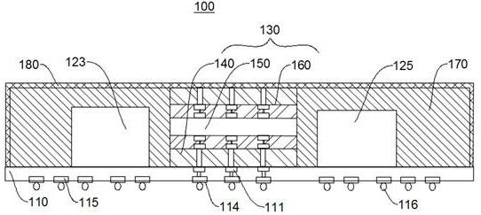
[0051] Please refer to figure 1 , the present embodiment provides a layered electromagnetic shielding packaging structure 100, including a module substrate 110, a shielding device 130 and a plurality of chips, the plurality of chips are arranged on the module substrate 110 at intervals, and at least two adjacent chips A shielding device 130 is provided between them. In this embodiment, the multiple chips include a second chip 123 and a third chip 125, the shielding device 130 includes a bottom shielding layer 140, an intermediate layer 150, and a top shielding layer 160 stacked, and the module substrate 110 is provided with a first contact. The point 111 is connected to a second ground point (not shown in the figure), the bottom shielding layer 140 is electrically connected to the first ground point 111 , and the top shielding layer 160 is electrically connected to the second ground point. The module substrate 110 is provided with a first package body 170 for plastic sealing ...

no. 2 example

[0063] An embodiment of the present invention provides a method for manufacturing a packaging structure, which mainly includes the following steps:

[0064] S100: Fabricate the shielding device 130. Wherein, the shielding device 130 includes a bottom shielding layer 140 , a middle layer 150 and a top shielding layer 160 .

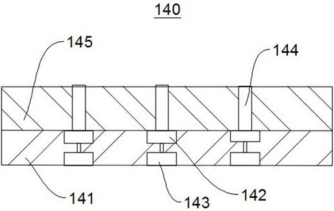
[0065] Please refer to Figure 5 , combined with figure 1 , S110: the steps of making the bottom shielding layer 140 and the top shielding layer 160 respectively include:

[0066] A first substrate 141 is provided, a first pad 142 is provided on the front side of the first substrate 141, a second pad 143 is provided on the reverse side of the first substrate 141, and the first pad 142 and the second pad 143 pass through the first substrate 141 The internal circuit is electrically connected. A metal post 144 is disposed on the first pad 142 , and the metal post 144 is used to electrically connect with the first ground point 111 or the second ground point. ...


PUM


Abstract

The application provides a layered electromagnetic shielding packaging structure and a manufacturing method of the packaging structure, which relate to the technical field of packaging. In the layered electromagnetic shielding packaging structure, the shielding device includes a bottom shielding layer, an intermediate layer and a top shielding layer stacked, a first grounding point and a second grounding point are arranged on the module substrate, and the bottom shielding layer and the first grounding point Electrically connected, the top shielding layer is electrically connected to the second grounding point; a first package is provided on the module substrate for plastic sealing of shielding devices and multiple chips, and a metal layer is provided on the outer surface of the first package. The bottom shielding layer and the top shielding layer are respectively electrically connected to the metal layer. By setting the layered shielding area, the top and bottom of the packaging structure can achieve the purpose of anti-electromagnetic interference, and the middle part of the packaging structure can weaken the electromagnetic shielding performance to meet the anti-interference requirements of different types of electronic products.

Description

technical field [0001] The invention relates to the field of packaging technology, in particular to a layered electromagnetic shielding packaging structure and a method for manufacturing the packaging structure. Background technique [0002] With the rapid development of the semiconductor industry, a system-in-a-package (SIP) module structure is widely used in the semiconductor industry. Moreover, as electronic products are widely used in high-frequency signals in the communication field, it is necessary to design anti-electromagnetic interference for electronic products. [0003] At present, electronic products are provided with partitioned electromagnetic shielding structures to prevent the occurrence of electromagnetic interference generated by various chips and components. The electromagnetic shielding structure often adopts the method of digging grooves in the package structure and filling them with conductive materials, through which the metal layer outside the packag...

Claims


Application Information

Patent Timeline
Patent Type & Authority Patents(China)
IPC IPC(8): H01L23/552H01L23/31H01L25/16H01L25/18H01L21/50H01L21/56
CPCH01L23/552H01L23/3107H01L25/16H01L25/18H01L21/50H01L21/561H01L2224/32145H01L2224/97
Inventor 孔德荣钟磊李利
Owner FOREHOPE ELECTRONICS NINGBO CO LTD
Why Eureka
Try Eureka