BGA electromagnetic shielding packaging structure and manufacturing method thereof

A packaging structure and electromagnetic shielding technology, which is applied in semiconductor/solid-state device manufacturing, circuits, electrical components, etc., can solve problems such as difficulty in meeting shielding requirements and poor quality of side sputtering

Inactive Publication Date: 2020-10-23
JCET GROUP CO LTD
View PDF4 Cites 0 Cited by
  • Summary
  • Abstract
  • Description
  • Claims
  • Application Information

AI Technical Summary

Problems solved by technology

[0010] The technical problem to be solved by the present invention is to provide a BGA electromagnetic shielding packaging structure and its manufacturing method in view of t

Method used


Image

  • BGA electromagnetic shielding packaging structure and manufacturing method thereof
  • BGA electromagnetic shielding packaging structure and manufacturing method thereof
  • BGA electromagnetic shielding packaging structure and manufacturing method thereof

Examples


Embodiment 1

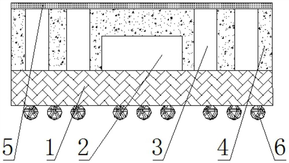
[0046] Such as figure 1 As shown, a BGA electromagnetic shielding package structure related to the present invention includes a substrate 1 on which a component 2 is mounted on the surface, and two rows of copper pillars 3 staggered inside and outside are arranged on the periphery of the component 2. The peripheral area of ​​the element 2 and the copper pillar 3 is encapsulated with a molding compound 4, the top of the copper pillar 3 is exposed on the upper surface of the molding compound 4, the upper surface of the molding compound 4 and the copper pillar 3 is provided with a sputtering layer 5, the substrate 1 A metal ball 6 is provided on the back;

[0047] The manufacturing method includes the following steps:

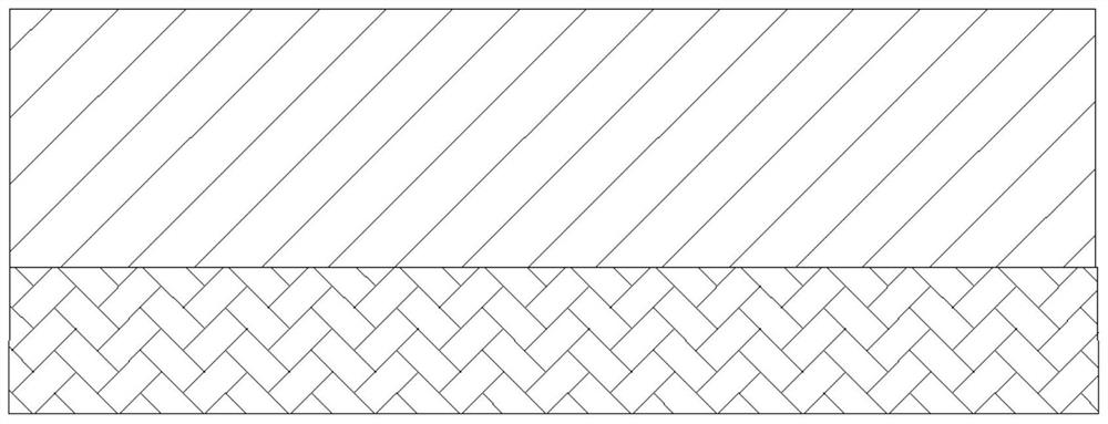
[0048] Step one, see figure 2 , Laying dry film on the surface of the substrate;

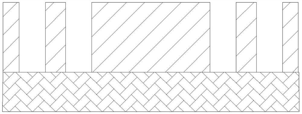
[0049] Step two, see image 3 , Expose and develop the dry film, remove part of the dry film, and expose the copper post area that needs to be electroplated later;

[0050] Step three, se...

Embodiment 2

[0060] Such as Picture 12 As shown, a BGA electromagnetic shielding package structure related to the present invention includes a substrate 1 on which a component 2 is mounted on the surface. The component 2 is provided with two rows of copper pillars 3 staggered inside and outside. The peripheral area of ​​the element 2 and the copper pillar 3 is encapsulated with a molding compound 4, the upper surface of the molding compound 4 is provided with an opening 7 at the corresponding position of the copper pillar 3, and the opening 7 exposes the top of the copper pillar 3. 4 The upper surface and the opening 7 are provided with a sputtering layer 5, the sputtering layer 5 is connected to the top of the copper pillar 3, and a metal ball 6 is provided on the back of the substrate 1;

[0061] The manufacturing method includes the following steps:

[0062] Step one, see Figure 13 , Lay dry film on the surface of the substrate;

[0063] Step two, see Picture 14 , Expose and develop the dr...


PUM


Abstract

The invention relates to a BGA electromagnetic shielding packaging structure and a manufacturing method thereof. The packaging structure comprises a substrate (1), wherein an element (2) is attached to the surface of the substrate (1); the periphery of the element (2) is provided with inner and outer rows of staggered copper columns (3), the peripheral areas of the element (2) and the copper columns (3) are encapsulated with a molding compound (4), the tops of the copper columns (3) are exposed out of the upper surface of the molding compound (4), the upper surfaces of the molding compound (4)and the copper columns (3) are provided with sputtering layers (5), and metal balls (6) are arranged at the back surface of the substrate (1). According to the BGA electromagnetic shielding packagingstructure and the manufacturing method thereof, the problems that the side sputtering quality of an existing product is poor, and the shielding requirement is difficult to meet can be solved.

Description

Technical field [0001] The invention relates to a BGA electromagnetic shielding packaging structure and a manufacturing method thereof, and belongs to the technical field of semiconductor packaging. Background technique [0002] During the sputtering process of the BGA product, the bottom solder ball needs to be protected to avoid the conduction of the sputtered metal layer and the bottom solder ball during the sputtering process to cause a short circuit. The existing technology solutions to this problem are: [0003] Step 1: Press the encapsulated whole product on the first protective film. The first protective film can protect the bottom pins or solder balls to prevent the bottom pins or solder balls from being plated during sputtering; [0004] Step 2: Cut the whole product into individual products; [0005] Step 3: Transfer a single product to the PI film, and arrange them on the PI film in an array with a certain interval; [0006] Step 4: Sputter the metal layer on the top surfa...

Claims


Application Information

Patent Timeline
IPC IPC(8): H01L23/552H01L23/31H01L21/56
CPCH01L23/552H01L23/3114H01L23/3128H01L21/56H01L2924/15311H01L2924/3025
Inventor 王杰
Owner JCET GROUP CO LTD
Why Eureka
Try Eureka