
Photoresist coating method and photoresist coating device

A coating device and coating method technology, applied in the field of photoresist coating method and device, can solve the problems of large wafer stress, uneven distribution of photoresist coating, poor coating of wafer edge, etc., to achieve Improved coating uniformity, reduced defects in edge distribution, and increased rotation speed

Pending Publication Date: 2021-01-22
SHANGHAI HUALI INTEGRATED CIRCUTE MFG CO LTD
View PDF0 Cites 2 Cited by
  • Summary
  • Abstract
  • Description
  • Claims
  • Application Information

AI Technical Summary

Problems solved by technology

[0005] The technical problems to be solved by the present invention are: uneven distribution in photoresist coating, excessive wafer stress due to rotation, poor coating of the edge of the wafer

Method used


Image

  • Photoresist coating method and photoresist coating device
  • Photoresist coating method and photoresist coating device
  • Photoresist coating method and photoresist coating device

Examples


Embodiment Construction

[0039] Specific embodiments of the present invention will be described in detail below in conjunction with the accompanying drawings.

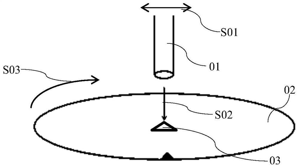
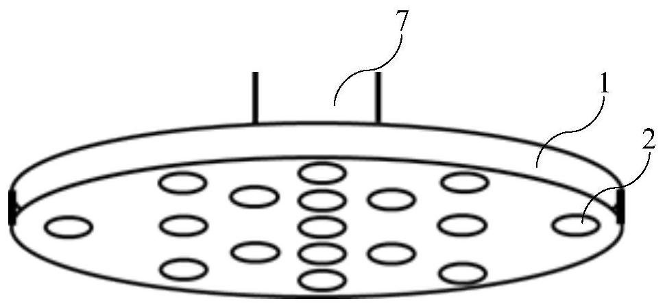
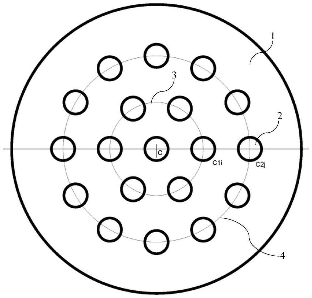
[0040] The photoresist coating method provided by the present invention includes: spraying photoresist at least two points above the wafer. According to the amount of photoresist ejected by each nozzle and the area that can be covered, a set number of photoresist ejection points are arranged above the wafer to cover the entire area of ​​the wafer. Moreover, the controllable arrangement of these points can improve the uniformity of the film thickness of the photoresist.

[0041] Furthermore, in the photoresist coating method provided by the present invention, points for spraying photoresist are provided at different radii in the center of the wafer. Accordingly, the requirement of uniformly spraying photoresist for wafer radii of different sizes can be met.

[0042] Further, the photoresist coating method provided by the present invention con...


PUM


Abstract

The invention provides a photoresist coating method. The photoresist coating method comprises the step of spraying photoresist at at least two points on the upper part of a wafer. The invention also provides a photoresist coating device, which comprises a spray disc, and at least two nozzles are arranged on the spray disc. Accordingly, the technical effects that the coating uniformity of the photoresist on the wafer can be improved, the photoresist coating device is suitable for wafers with larger sizes, the whole wafer can be covered, the defect that the edge of the wafer cannot be distributed on photoresist distribution is reduced, rotation is not needed or the rotation speed is not increased are achieved, and the photoresist coating device is suitable for large-scale production. And thewafer is prevented from being thrown out or broken due to stress generated by centrifugal action.

Description

technical field [0001] The invention relates to the field of integrated circuit manufacturing, in particular to a photoresist coating method and device. Background technique [0002] In the field of integrated circuit manufacturing, one of the important process steps is to coat photoresist on the wafer. refer to figure 1 As shown, in the prior art, the photoresist coating method is: first step, S01 moves photoresist nozzle 01 (nozzle) to the center of wafer 02; second step, S02 sprays photoresist 03 onto The center of the wafer 02; the third step, S03, and then the photoresist 03 is evenly cured on the wafer 02 with a certain film thickness through rotation. [0003] The increase in wafer size means that the same process steps can produce more chips, thereby reducing the cost of transistors. However, the increase in wafer size requires higher requirements for equipment, such as in terms of uniformity. With the advancement of integrated circuit manufacturing technology, p...

Claims


Application Information

Patent Timeline
IPC IPC(8): G03F7/16
CPCG03F7/16
Inventor 李飞李文亮吴鹏
Owner SHANGHAI HUALI INTEGRATED CIRCUTE MFG CO LTD
Learn More