Polysilazane, method of synthesizing polysilazane, composition for manufacturing semiconductor device, and method of manufacturing semiconductor device using the composition

a polysilazane and polysilazane technology, applied in semiconductor devices, solid-state devices, electrical devices, etc., can solve the problems of a manufacturing process for semiconductor devices, a large amount of polysilazane, etc., to achieve excellent groove-filling properties and high molecular weight

Inactive Publication Date: 2010-05-06
KOREA KUMHO PETROCHEMICAL CO LTD
View PDF1 Cites 17 Cited by
  • Summary
  • Abstract
  • Description
  • Claims
  • Application Information

AI Technical Summary

Benefits of technology

[0009]An aspect of the present invention provides polysilazane excellent in a groove-filling property while having a relatively high molecular weight, a method of synthesizing

Problems solved by technology

In this case, problems may be created on a process for manufacturing the semiconductor device.
However, in a process for manufacturing the semiconductor device including the trench having a width of about 60 run or less according to the design rule, pores may be disadvantageously formed inside the trench when using the CVD method for the purpose of forming the silicon oxide layer inside the trench.
However, the polysilazane obtained through the above-mentioned reaction may have disadvantages that a molecular weight of the polysilazane is extraordinarily s

Method used


Image

  • Polysilazane, method of synthesizing polysilazane, composition for manufacturing semiconductor device, and method of manufacturing semiconductor device using the composition
  • Polysilazane, method of synthesizing polysilazane, composition for manufacturing semiconductor device, and method of manufacturing semiconductor device using the composition
  • Polysilazane, method of synthesizing polysilazane, composition for manufacturing semiconductor device, and method of manufacturing semiconductor device using the composition

Examples


synthesis examples

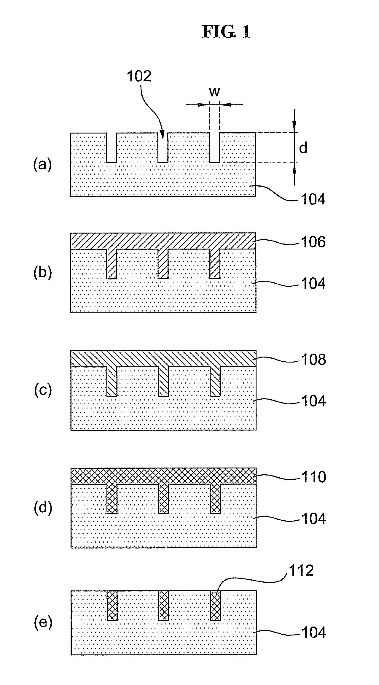
[0065]1. Polysilazane Synthesis

[0066]Synthesis Example 1

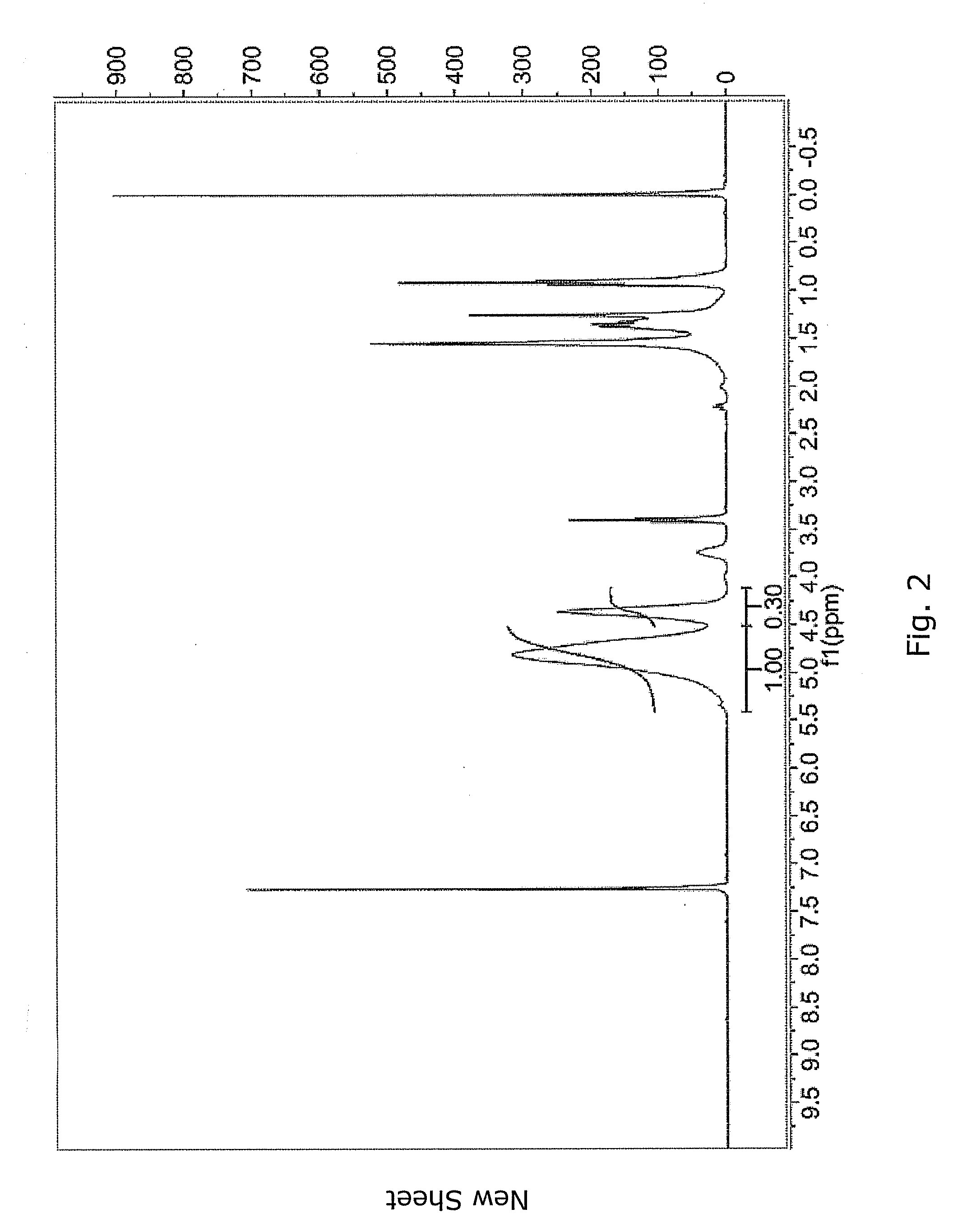
[0067]About 500 g of dried pyridine was inserted in a flask, cooled to 0° C. or less, and then about 35 g of dichlorosilane and about 4.7 g of trichlorosilane were gradually added in the flask. Subsequently, about 10 g of ammonia was gradually added in the flask, and stirred at an identical temperature about for one hour. Next, about 1.1 g of hydroxylamine was added in the flask, stirred at room temperature for about two hours, and then a residual of the ammonia was removed using a nitrogen gas. Next, an ammonium salt existing in a reaction mixture from which the ammonia is removed was removed using a filter. Next, the pyridine was completely removed from a remainder in a vacuum condition, thereby obtaining about 12.8 g of polysilazane A (see Reaction formula 1 below). A polystyrene conversion weight average molecular weight of the obtained polysilazane A was about 3,200. An 1H-NMR spectrum of the polysilazane A is shown in FIG...

synthesis example 2

[0069]About 14.6 g of polysilazane B was obtained through the same process as that of the above Synthesis example 1, excepting that the pyridine was heated to about 100° C. at an atmospheric pressure, and thus removed from the remainder. A polystyrene conversion weight average molecular weight of the obtained polysilazane B was about 25,000.

synthesis example 3

[0070]About 13.6 g of polysilazane C was obtained through the same process as that of the above Synthesis example 1, excepting that about 2.4 g of the trichlorosilane was used instead of about 4.7 g of the trichlorosilane. A polystyrene conversion weight average molecular weight of the obtained polysilazane C was about 6,000.


PUM

PropertyMeasurementUnit
Temperatureaaaaaaaaaa

Abstract

Disclosed are polysilazane, a method of synthesizing the polysilazane, a composition for manufacturing a semiconductor device, and a method of manufacturing a semiconductor device using the composition. The polysilazane is synthesized through a reaction, under a catalyst, between dichlorosilane, trichlorosilane, and ammonia added in a reaction solvent as a reactant. In this instance, a polystyrene conversion weight average molecular weight of the polysilazane is about 2,000 to 30,000.

Description

CROSS-REFERENCE TO RELATED APPLICATION[0001]This application claims the benefit of Korean Patent Application No. 10-2008-0109287, filed on Nov. 5, 2008, in the Korean Intellectual Property Office, the disclosure of which is incorporated herein by reference.BACKGROUND OF THE INVENTION[0002]1. Field of the Invention[0003]The present invention relates to polysilazane, a method of synthesizing the polysilazane, a composition for manufacturing a semiconductor device, and a method of manufacturing a semiconductor device using the composition.[0004]2. Description of Related Art[0005]In general, a semiconductor device may include patterns formed on a silicon wafer, for example, patterns such as a transistor, a bit line, a capacitor, a metal line, and the like. Because these patterns may be conductive, an insulating layer may be formed between these patterns. A process for forming the insulating layer may include a Premetal Dielectric (PMD) process for insulating between the transistor and b...

Claims


Application Information

Patent Timeline
IPC IPC(8): H01L51/30C08G77/12
CPCC08G77/62H01L21/02164H01L21/02222H01L21/02282H01L21/3125H01L21/316C08L83/16H01L21/20
Inventor PARK, JOO HYEONCHANG, YONG
Owner KOREA KUMHO PETROCHEMICAL CO LTD
Why Eureka
Try Eureka