Liquid crystal display device

a liquid crystal display and display film technology, applied in the field of liquid crystal display devices, can solve the problems of low alignment stability, poor quality display, power-quality display typified, etc., and achieve the effects of avoiding degrading the mechanical enhancing the anchoring strength of the alignment film, and enhancing the film strength

Active Publication Date: 2011-08-18
JAPAN DISPLAY INC +1
View PDF9 Cites 82 Cited by
  • Summary
  • Abstract
  • Description
  • Claims
  • Application Information

AI Technical Summary

Benefits of technology

According to the present invention, the alignment film has the two-layer structure including the photo-alignment film adjoining liquid crystals and the alignment film with enhanced film strength adjoining the substrate. Therefore, by way of photo-alignment, it is possible realize a liquid crystal display device in which the azimuthal anchoring strength is strong and

Problems solved by technology

Low alignment stability varies an initial LC alignment direction, resulting in a poor-quality display.
Especially, in an LCD device using an IPS type LCD panel for which high alignment stability is required, low alignment stability tends to give rise to a power-quality display ty

Method used


Image

  • Liquid crystal display device
  • Liquid crystal display device
  • Liquid crystal display device

Examples


first embodiment

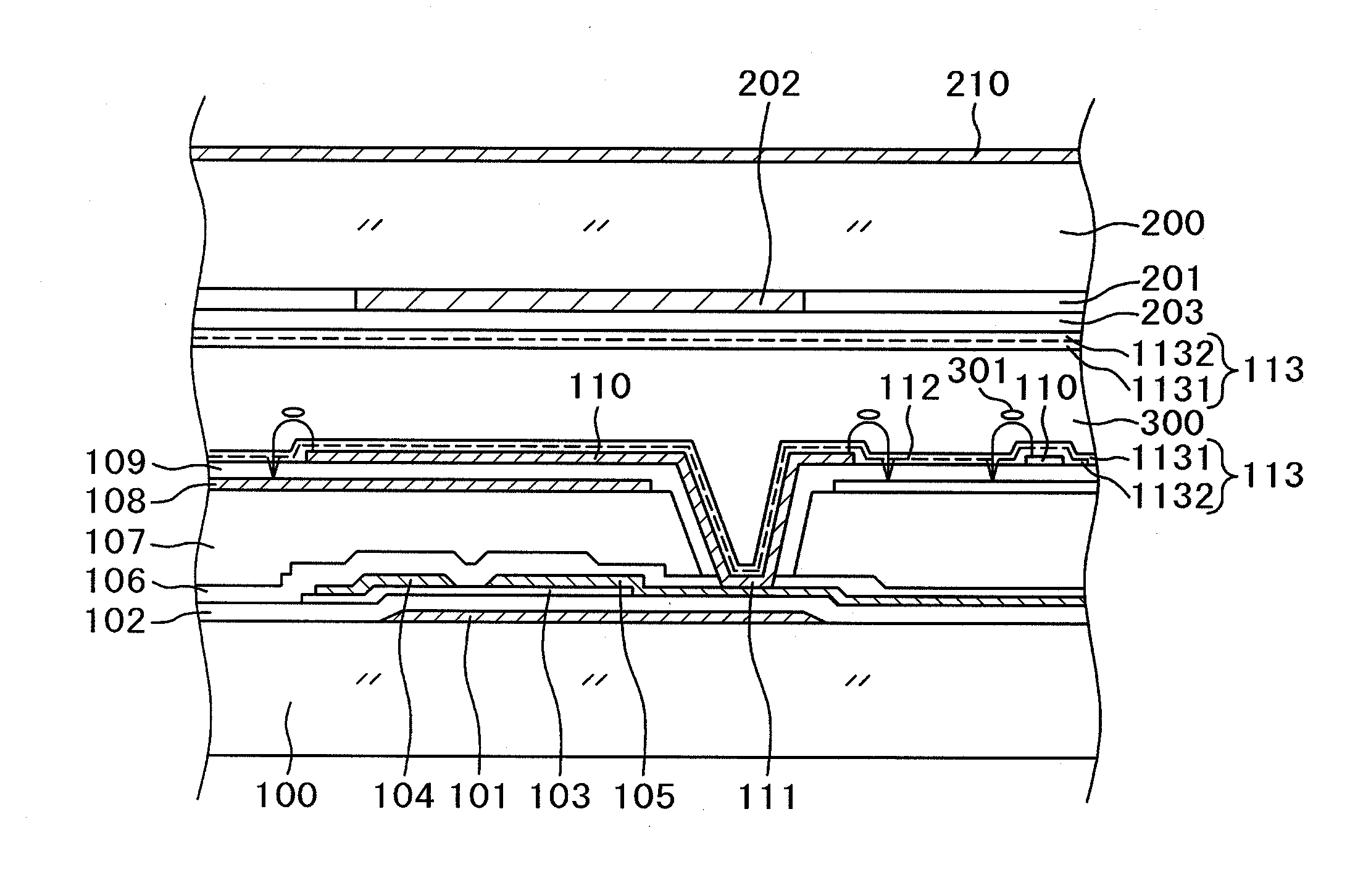
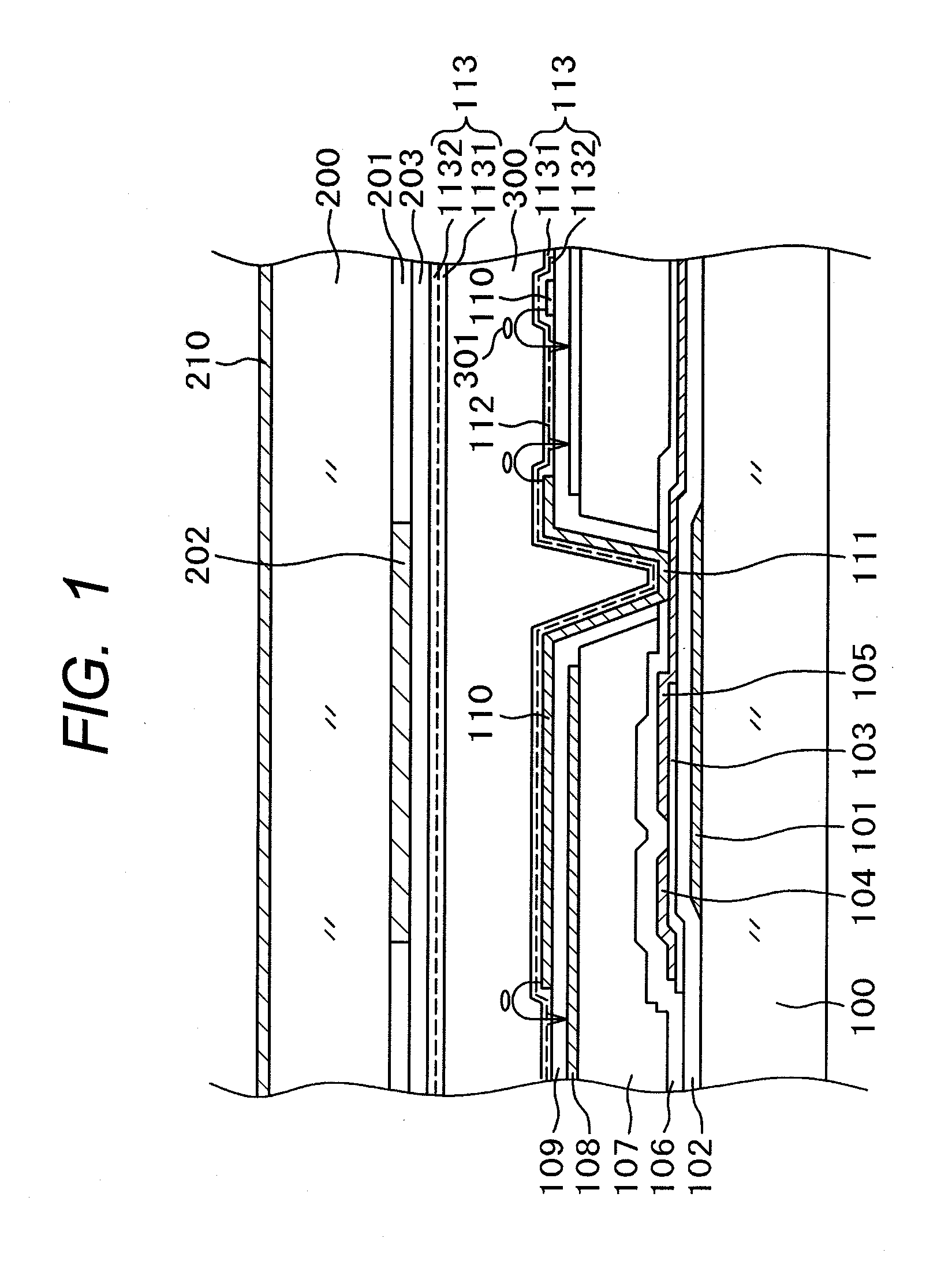
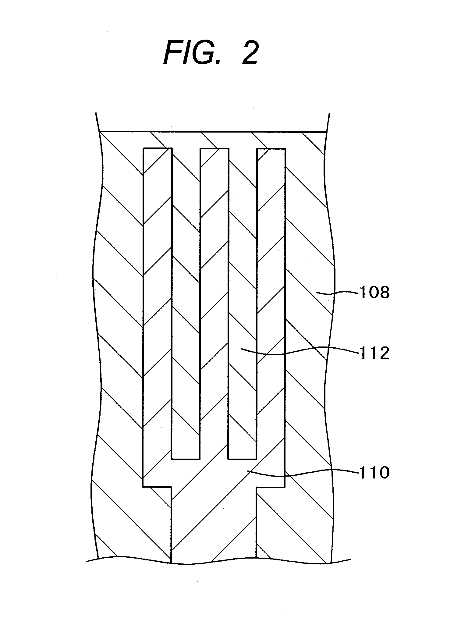
FIG. 1 is a cross-sectional diagram showing a structure in a display region of an IPS type liquid crystal display device. A variety of electrode structures for IPS type liquid crystal display devices are proposed and put in practical use. The structure shown in FIG. 1 is widely used now. In simple terms, over a common electrode 108 formed in a flat monolithic form, a comb-shaped pixel electrode 110 is formed with an insulation layer intervening therebetween. By rotating liquid crystals 301 depending on a voltage between the pixel electrode 110 and the common electrode 108, light transmissibility through a liquid crystal layer 300 is controlled pixel by pixel and an image is thus produced. The structure in FIG. 1 will be described in detail below. While the present invention is described by taking the structure in FIG. 1 as an example, the invention can be applied to an IPS type liquid crystal display device having a structure other than that shown in FIG. 1.

In FIG. 1, a gate electro...

second embodiment

In the first embodiment, how the alignment film structure and the process for photo-alignment contribute to an advantageous effect against AC afterimages is mainly discussed. The structure of the present invention can achieve the effect against so-called DC afterimages, besides AC afterimages.

DC afterimages are a phenomenon resulting from charge accumulation in certain portions of the alignment film. Hence, DC afterimages are a reversible phenomenon, because they disappear when charges dissipate. In order to avoid DC afterimages, it is conceivable that the alignment film is adapted to have a structure that facilitates fast dissipation of charges accumulated in the alignment film or a structure that primarily prevents charges from being accumulated in the alignment film.

First, descriptions are provided for the structure that facilitates fast dissipation of accumulated charges. We evaluated DC afterimages as follows. That is, the checker flag pattern made up of 8×8 white and black cel...


PUM

PropertyMeasurementUnit
Temperatureaaaaaaaaaa

Abstract

This invention enables forming a photo-alignment film having a large LC anchoring strength in an IPS type liquid crystal display device. An alignment film is adapted to have a two-layer structure including a photo-alignment film and an alignment film with enhanced film strength. The photo-alignment film is formed of a precursor of polyamide acid ester, 80 percent or more of which is polyamide acid ester including cyclobutane. The alignment film with enhanced film strength is formed of a precursor of polyamide acid. After irradiating the substrate with ultraviolet light for photo-alignment, the substrate is heated. Thus, it is possible to achieve a high LC anchoring strength of the alignment film as the whole for photo-alignment, without degrading the mechanical strength of the alignment film with enhanced film strength.

Description

CLAIM OF PRIORITYThe present application claims priority from Japanese Patent Application JP 2010-032443 filed on Feb. 17, 2010, the content of which is hereby incorporated by reference into this application.FIELD OF THE INVENTIONThe present invention relates to a liquid crystal display device and particularly to a liquid crystal display device including a liquid crystal display panel in which alignment films are provided with the capability of liquid crystal (LC) alignment control by light irradiation.BACKGROUND OF THE INVENTIONIn a liquid crystal display (LCD) device, a TFT substrate over which pixel electrodes and thin-film transistors, inter alia, are formed in a matrix and an opposing substrate over which color filters, inter alia, are formed in positions corresponding to the pixel electrodes in the TFT substrate are placed facing each other and liquid crystals are sandwiched between the TFT substrate and the opposing substrate. An image is produced by controlling light transmi...

Claims


Application Information

Patent Timeline
IPC IPC(8): G02F1/1337H01L33/08
CPCG02F1/133723G02F1/133711G02F1/134363G02F1/133788C09K2323/00C09K2323/02C09K19/56G02F1/1368H01L27/1262H01L27/1296
Inventor KUNIMATSU, NOBORUMATSUI, CHIKAESONODA, HIDEHIROMATSUMOTO, YUKOUCHINO, SHOICHIMATSUMORI, MASAKITOMIOKA, YASUSHI
Owner JAPAN DISPLAY INC
Why Eureka
Try Eureka