Eureka AIR delivers breakthrough ideas for toughest innovation challenges, trusted by R&D personnel around the world.

Semiconductor epoxy resin packaging equipment

A technology of epoxy resin and packaging equipment, which is applied in semiconductor/solid-state device manufacturing, electrical components, circuits, etc. It can solve the problem that semiconductors are prone to movement, etc., and achieve the effect of shortening packaging time and improving quality

Inactive Publication Date: 2021-01-29
谭秀美
View PDF5 Cites 1 Cited by
  • Summary
  • Abstract
  • Description
  • Claims
  • Application Information

AI Technical Summary

Problems solved by technology

[0003] The technical problem to be solved by the present invention is to provide a semiconductor epoxy resin encapsulation equipment, which solves the problem of easy movement during semiconductor encapsulation

Method used


Image

  • Semiconductor epoxy resin packaging equipment
  • Semiconductor epoxy resin packaging equipment
  • Semiconductor epoxy resin packaging equipment

Examples


Embodiment Construction

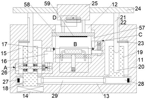
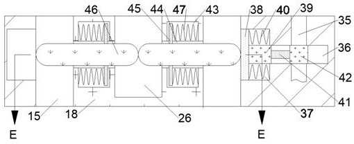
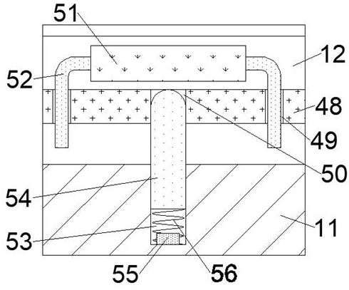
[0021] Combine below Figure 1-6 The present invention is described in detail, wherein, for the convenience of description, the orientations mentioned below are defined as follows: figure 1 The up, down, left, right, front and back directions of the projection relationship itself are the same.

[0022] combined with Figure 1-6 The described semiconductor epoxy resin encapsulation equipment includes an encapsulation body 11, the upper end of the encapsulation body 11 is communicated with an encapsulation chamber 12 with an upward opening, and the underside of the encapsulation chamber 12 is provided with a pulley chamber 13. The inside of the pulley chamber 13 is provided with a transmission device, and the left and right sides of the packaging chamber 12 on the upper side of the pulley chamber 13 are symmetrically provided with a control chamber 15, and the lower wall of the control chamber 15 on the left side is rotated with a belt penetrating through the belt. The main ro...


PUM


Abstract

Semiconductor epoxy resin packaging equipment is disclosed in the invention, and comprises a packaging machine body, a packaging cavity with an upward opening is formed in the upper end face of the packaging machine body in a communicating mode, a belt wheel cavity is formed in the lower side of the packaging cavity, a transmission device is arranged in the belt wheel cavity, and control cavitiesare symmetrically formed in the positions, on the upper side of the belt wheel cavity, of the left side and the right side of the packaging cavity. A main rotating shaft penetrating through the upperwall face and the lower wall face of the left side of the belt wheel cavity is rotationally arranged on the lower wall face of the left control cavity. An semiconductor element is placed in the equipment, the semiconductor is positioned by using the pins of the semiconductor, the covering amount of the epoxy resin can be effectively controlled through the combination of the lifting of an upper pressing plate and the release of epoxy resin, and the curing speed of the epoxy resin is improved through the accelerated curing treatment of the epoxy resin, so the quality of cured epoxy resin is effectively improved, the semiconductor packaging time is shortened, the situation that the service life of a semiconductor is affected by vibration and oxidation is effectively enhanced, and the qualityof the semiconductor is improved.

Description

technical field [0001] The invention relates to the technical field of semiconductors, in particular to semiconductor epoxy resin packaging equipment. Background technique [0002] Semiconductor packaging is to cover the lines arranged on the semiconductor, effectively avoiding the contact between the semiconductor lines and the air, and reducing the aging speed of the lines. In the existing semiconductor packaging technology, due to the small size and light weight of the semiconductor, it is not easy to fix during the packaging process, which causes the semiconductor to move during packaging, which affects the thickness of the semiconductor package, which in turn affects the heat dissipation of the semiconductor, and also affects the subsequent installation process of the semiconductor. , The uneven thickness during the semiconductor packaging process has a greater impact on the packaging of the product. Contents of the invention [0003] The technical problem to be ...

Claims


Application Information

Patent Timeline
IPC IPC(8): H01L21/68H01L21/56
CPCH01L21/68H01L21/565
Inventor 谭秀美
Owner 谭秀美
Why Eureka
Eureka Blog
Learn More