A High Power High Voltage Schottky Barrier Diode

A Schottky potential and diode technology, applied in the field of diodes, can solve problems such as the reduction of SSG capability, and achieve the effects of high SSG capability, reduced resistance, and high ESD capability

Active Publication Date: 2021-07-23
YANGZHOU GUOYU ELECTRONICS
View PDF16 Cites 0 Cited by
  • Summary
  • Abstract
  • Description
  • Claims
  • Application Information

AI Technical Summary

Problems solved by technology

However, there is a contradiction between ESD and SSG of traditional high-power high-voltage Schottky barrier diodes, that is, improving ESD capability will lead to a decrease in SSG capability, and vice versa

Method used


Image

  • A High Power High Voltage Schottky Barrier Diode
  • A High Power High Voltage Schottky Barrier Diode
  • A High Power High Voltage Schottky Barrier Diode

Examples


Embodiment 1

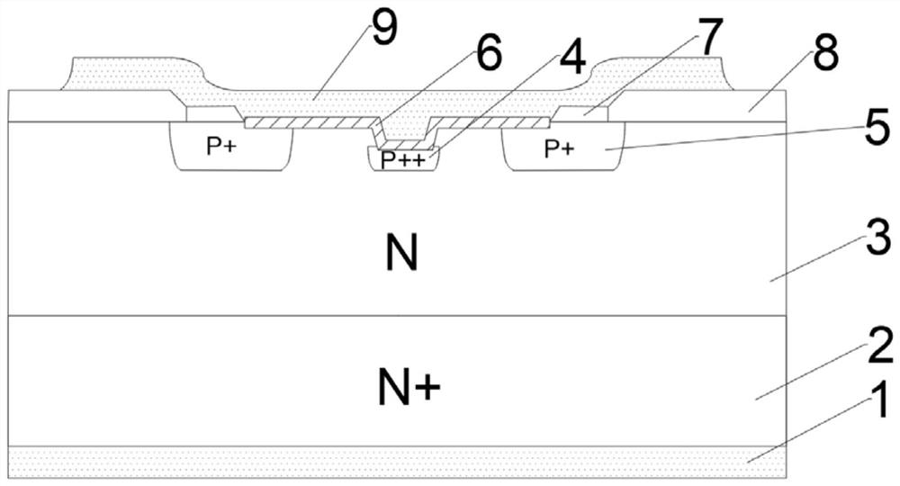
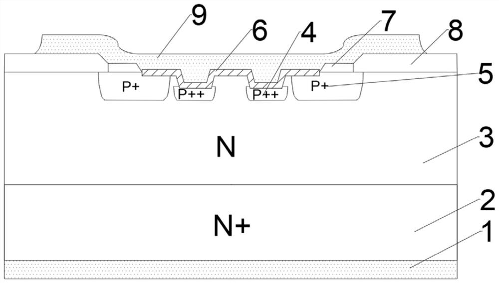
[0040] like Figure 1-2 As shown, a high-power high-voltage Schottky barrier diode, including from bottom to top: back metal layer 1, N+ substrate 2, N epitaxial layer 3, metal silicide layer 6, front metal layer 9; N epitaxial layer The upper part of 3 is provided with a heavily doped anode region 4 and a P+ guard ring 5, the guard ring 5 is arranged around the heavily doped anode region 4, a groove is opened on the upper surface of the N epitaxial layer 3, and the heavily doped anode region 4 is arranged in the groove At the bottom of the groove, the metal silicide layer 6 is arranged along the groove, the upper surface of the heavily doped anode region 4 and the guard ring 5 are in contact with the lower surface of the metal silicide layer 6, and the heavily doped anode region 4 at the bottom of the groove cooperates with the The metal silicide layer 6 and the front metal layer 9 form an independent ESD discharge area; a thin oxygen layer 7 is set between the guard ring 5 a...

Embodiment 2

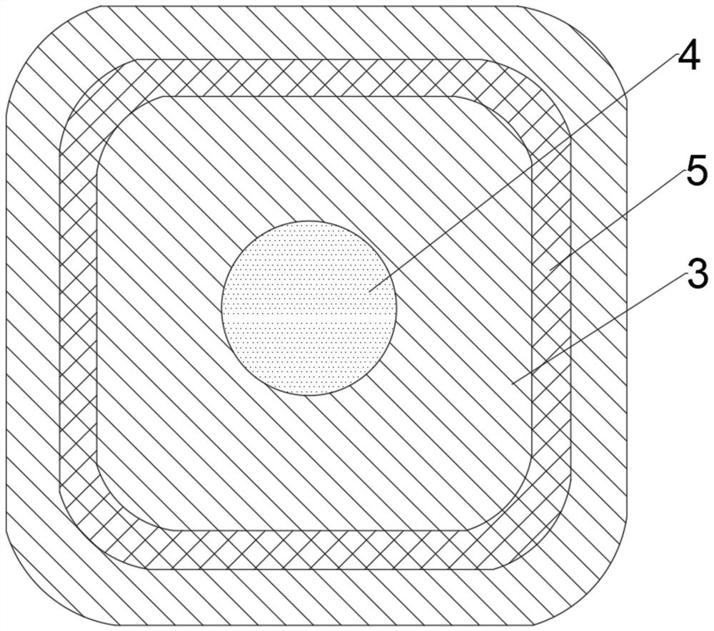
[0043] like Figure 3-4 As shown, a high-power high-voltage Schottky barrier diode, on the basis of the first embodiment, the area surrounded by the guard ring 5 is the active area, the active area is rectangular, and the corners of the active area are arc-shaped, There are four heavily doped anode regions 4 and they are distributed at the corners of the active region. The heavily doped anode regions 4 are fan-shaped and have a radius greater than that of the arc at the corners of the active region.

[0044] The above-mentioned technical solutions in the embodiments of the present application have at least the following technical effects or advantages:

[0045] 1. The upper part of the N epitaxial layer is provided with a heavily doped anode area, which forms an independent ESD discharge area in conjunction with the metal silicide layer and the front metal layer. This structure sets an independent ESD discharge area in the diode active area to reduce the impact on The influen...

Embodiment 3

[0049] A kind of diode preparation method that realizes the structure of above-mentioned embodiment, comprises the following steps:

[0050] Step 1: forming an N epitaxial layer on an N+ substrate;

[0051] Step 2: forming field oxygen on the N epitaxial layer;

[0052] Step 3: Form a protective ring and thin oxygen on the N epitaxial layer and field oxygen by photolithography, etching, implantation, glue removal, and annealing;

[0053] Step 4: forming grooves on the N epitaxial layer and field oxygen by photolithography and etching;

[0054] Step 5: Forming a heavily doped anode under the trench in the N epitaxial layer by implantation, glue removal, and annealing;

[0055] Step 6: Form contact holes on the N epitaxial layer, field oxygen, thin oxygen, and grooves by photolithography, etching, and glue removal, for forming metal silicide layer windows;

[0056] Step 7: forming a metal silicide layer on the contact hole by depositing a barrier metal layer, rapid thermal an...


PUM


Abstract

The invention discloses a high-power high-voltage Schottky barrier diode in the technical field of diodes, comprising: a back metal layer; an N+ substrate, the N+ substrate is arranged above the back metal layer; an N epitaxial layer, and the N epitaxial layer is arranged on Above the N+ substrate, a heavily doped anode region is provided on the upper part of the N epitaxial layer; a metal silicide layer, the metal silicide layer is arranged above the N epitaxial layer, and the metal silicide layer is in contact with the heavily doped anode region; the front metal layer, the front The metal layer is disposed above the metal silicide layer and covers the metal silicide layer. The heavily doped anode region of the diode cooperates with the metal silicide layer and the front metal layer to form an independent ESD discharge region, which reduces the impact on the SSG capability of the diode and enables the chip to obtain extremely high ESD capability and SSG capability at the same time, thereby The reliability of the device is greatly improved.

Description

technical field [0001] The invention relates to the technical field of diodes, in particular to a high-power high-voltage Schottky barrier diode. Background technique [0002] The Schottky barrier diode is named after its inventor, Dr. Schottky, which uses the metal-semiconductor junction principle formed by the contact of metal and semiconductor. Therefore, SBD is also called metal-semiconductor (contact) diode or surface barrier diode, which is a single carrier diode. [0003] At present, high-power high-voltage Schottky barrier diodes are gradually developing towards high reliability. The reliability of high-power high-voltage Schottky barrier diodes has been valued by more and more customers. Typical reliability indicators include HTRB, PCT, IFSM, ESD, SSG, etc. Among them, ESD capability and SSG capability are especially concerned by high-voltage and high-power SBD customers. However, there is a contradiction between ESD and SSG of traditional high-power high-voltage ...

Claims


Application Information

Patent Timeline
Patent Type & Authority Patents(China)
IPC IPC(8): H01L29/872H01L21/329H01L29/06
CPCH01L29/0603H01L29/0615H01L29/0684H01L29/66257H01L29/872
Inventor 马文力李浩徐婷
Owner YANGZHOU GUOYU ELECTRONICS
Why Eureka
Try Eureka