A visual inspection method for IC defects in transparent packaging

A visual inspection and defect technology, applied in the field of inspection, can solve the problems of high workload of workers, low inspection efficiency, poor stability of inspection results, etc., and achieve the effect of improving production efficiency and production quality, high inspection efficiency and fast inspection speed.

Active Publication Date: 2021-08-31
高视科技(苏州)股份有限公司
View PDF7 Cites 0 Cited by
  • Summary
  • Abstract
  • Description
  • Claims
  • Application Information

AI Technical Summary

Problems solved by technology

[0004] (1) The manual visual inspection method cannot achieve 24h uninterrupted work, and the work intensity of workers is high, which is easy to cause visual fatigue, lead to false detection, and directly reduce the reliability of product detection;
[0005] (2) The quality judgment standard of manual visual inspection is not easy to quantify, resulting in poor stability of test results;
[0006] (3) Due to the small size of IC integrated chips, limited by the recognition ability of human eyes, the detection speed and accuracy of manual visual inspection are low, resulting in low detection efficiency and high labor costs
[0008] However, the detection speed, detection efficiency and detection accuracy of the above-mentioned fast detection method still need to be improved. For this reason, the present invention provides a visual detection method for the defects of transparent packaged ICs

Method used


Image

  • A visual inspection method for IC defects in transparent packaging
  • A visual inspection method for IC defects in transparent packaging
  • A visual inspection method for IC defects in transparent packaging

Examples


Embodiment 1

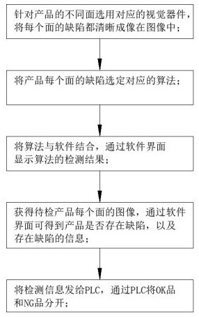
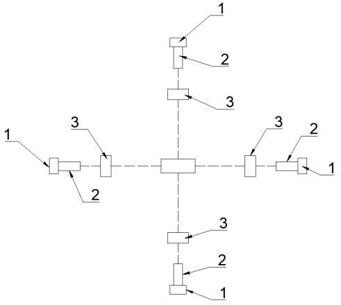
[0029] see Figure 1-Figure 2 , the visual detection method of the transparent encapsulation IC defect of the present invention, comprises the following steps;

[0030] (1) Place the product to be tested on the testing equipment, and select different visual devices according to the different sides of the product to collect the image information of each side of the product, and upload the collected image information to the processor ;

[0031] (2) After the processor receives the image information, it compares the image information with the standard image of OK products to find out the defective products, and selects the corresponding algorithm for the defects existing in each surface of the product. The process is as follows:

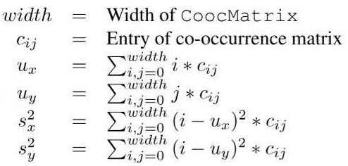
[0032] Firstly, according to the differences in the background on the texture of the image information, the gray level co-occurrence matrix is ​​used to calculate the following four different texture representation features in the image information: ...

Embodiment 2

[0059] In this embodiment, a specific case is used to illustrate the visual inspection method for the defect of a transparent packaged IC of the present invention:

[0060] Taking the scratch on the front as an example, after the visual device in Example 1 detects that there is a defect on the front of the product, the algorithm can detect that there is a defect in a specific area on the front of the product, but it is not sure what kind of defect it is, because There are still defects such as dirt and air bubbles on the front side. At this time, it can be judged according to the shape and gray value changes of the defects. For example, air bubbles and scratches will cause the local gray value to increase, and dirt will cause the local gray value to decrease. , and the bubbles are usually round, the scratches are linear, and the dirt has no fixed shape. At this time, if the algorithm judges that the defect causes the local gray value to become higher, and the defect is linear,...


PUM


Abstract

The invention discloses a visual inspection method for defects in a transparent packaged IC. Firstly, a product to be inspected is placed on an inspection device, and different visual devices are selected according to each surface of the product to collect image information of each surface of the product. And upload it to the processor; the processor compares the image information with the standard image of the OK product, finds out the defective product, and selects the corresponding algorithm for each defect of the product according to the shape of the defect in the image; Extract the defect features of each surface of the product to judge the shape and location of the defect; then use the algorithm to detect again to obtain the specific information of the product OK and NG, as well as the defect type of the NG product; finally the processor will The product information obtained by testing is sent to PLC, and PLC accurately separates OK and NG products. The visual detection method of the present invention can quickly realize the detection of transparent packaged ICs, and has faster detection speed, higher detection efficiency and detection accuracy.

Description

technical field [0001] The invention relates to a detection method, in particular to a visual detection method for the defect of a transparent packaged IC. Background technique [0002] Semiconductor integrated circuits are active components such as transistors, diodes, and passive components such as resistors and capacitors, interconnected according to a certain circuit, and "integrated" on a single semiconductor chip to complete specific circuit or system functions. The scale of the IC industry in mainland China is relatively small, accounting for only a small part of the global IC industry. Generally speaking, China's IC industry lags behind the international advanced level in terms of economy and technology. In recent years, the State Council has issued relevant documents on the development of the IC industry, which has stimulated investment in the domestic IC industry to a certain extent, thereby promoting the growth rate of China's IC industry. [0003] At present, th...

Claims


Application Information

Patent Timeline
Patent Type & Authority Patents(China)
IPC IPC(8): G06T7/00G06T7/45
CPCG06T7/0004G06T2207/30148G06T7/45
Inventor 邹双盛邹伟金徐武建周波
Owner 高视科技(苏州)股份有限公司
Why Eureka
Try Eureka