

Glass photonic crystal selective wave absorber based on DBS algorithm
A photonic crystal and selective technology, applied in optics, instruments, mirrors, etc., can solve the problem of poor radiation cooling effect of devices, and achieve the effect of solving the problem of multi-layer loss, single material, and excellent performance
- Summary
- Abstract
- Description
- Claims
- Application Information
AI Technical Summary
Problems solved by technology
Method used
Image

Examples
Embodiment Construction
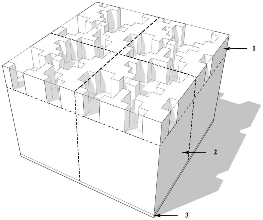
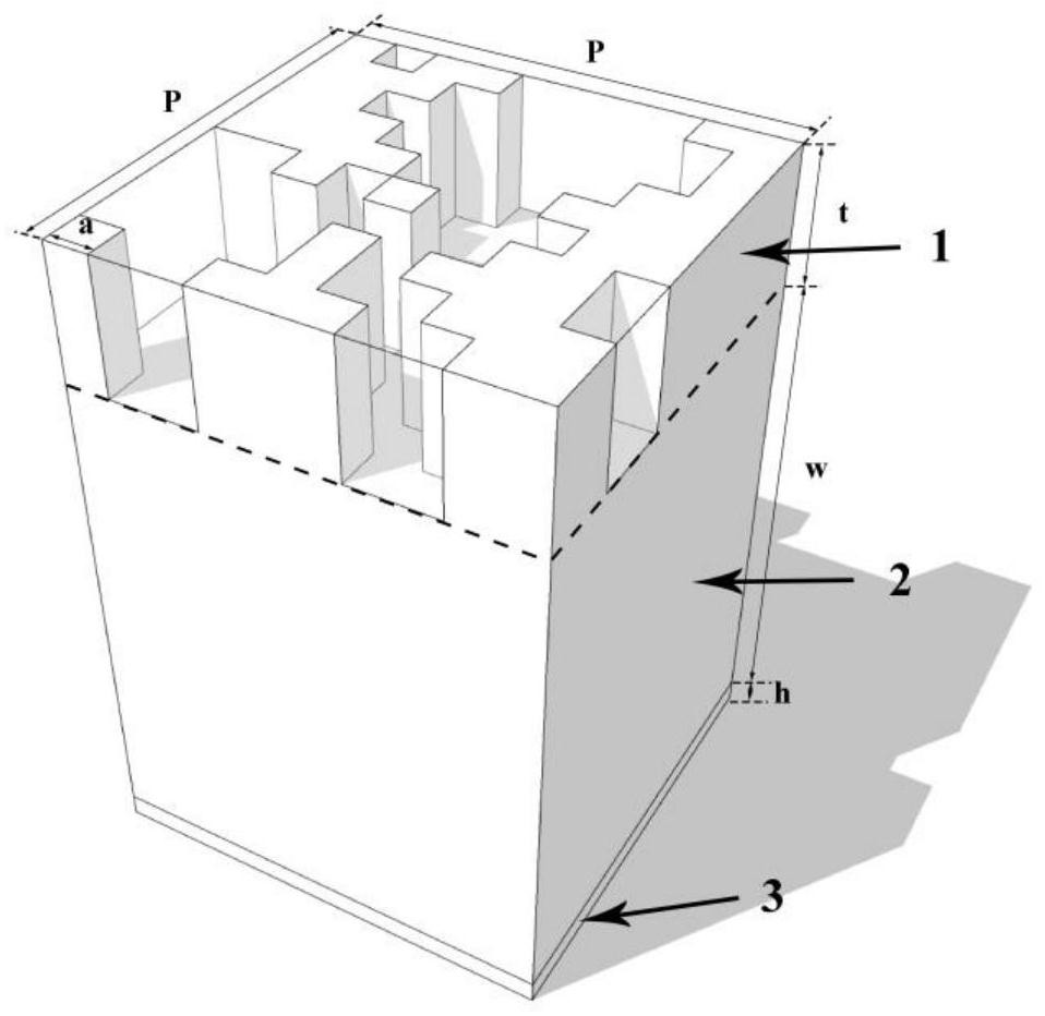
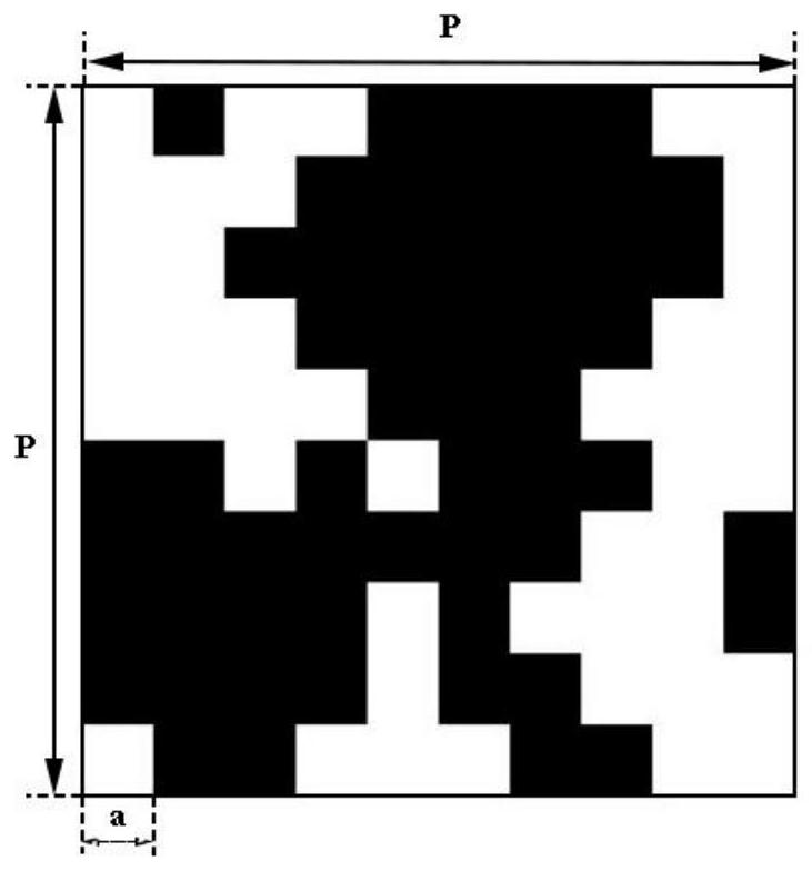
[0025] The present invention proposes a glass photonic crystal selective absorber based on the DBS algorithm, and its periodic three-dimensional structure schematic diagram is as follows figure 1 As shown, the schematic diagram of the three-dimensional structure of a unit in the periodic structure is shown in figure 2 As shown, it includes an optimized selective absorption region 1, an absorption layer 2, and a reflection layer 3.
[0026] The material of the optimized selective absorption region 1 is glass photonic crystal, and the thickness of the optimized selective absorption region 1 is t=3 μm; the material of the described absorption layer 2 is silicon dioxide, and the thickness of the absorption layer 2 is w=11 μm, the material of the reflective layer 3 is silver, and the thickness is h=0.5 μm.
[0027] Silver is widely used as an ideal conductor material in the infrared band, so we coat a layer of silver film on the bottom of the silicon dioxide absorbing layer, so t...
PUM
| Property | Measurement | Unit |
|---|---|---|
| Size | aaaaa | aaaaa |
Abstract
Description
Claims
Application Information