MOSFET gate-source voltage interference conduction path model

A technology of conduction path, gate-source voltage, applied in CAD circuit design, complex mathematical operation, design optimization/simulation, etc., can solve the problems of increasing converter loss, lack of explanation of interference oscillation, breakdown of gate electrolyte, etc. The effect of simplified calculation, intuitive physical meaning, concise mathematical representation

Active Publication Date: 2021-03-02
BEIJING JIAOTONG UNIV +1
View PDF18 Cites 1 Cited by
  • Summary
  • Abstract
  • Description
  • Claims
  • Application Information

AI Technical Summary

Problems solved by technology

However, for the second type of conducted interference, there is still a lack of systematic theoretical guidance and engineering design solutions in the field of power electronics
[0003] In the second type of conducted interference, drastic changes in the drain-source voltage and current are conducted through the Miller capacitance, causing spikes and oscillations in the gate-source voltage, affecting the stability of the gate-source voltage, which will increase the loss of the converter, and even cause the bridge arm to pass through, The breakdown of gate electrolyte seriously threatens the performance improvement and safe and reliable application of MOSFET
However, these complex mechanism models only consider the voltage spikes caused by disturbances, and lack explanations for disturbance oscillations; moreover, in the modeling process, too many non-dominant stray parameters are introduced
Therefore, using these complex mechanism models, it is still difficult to directly face engineering applications and give design guidelines considering gate pressure stress; the method of reducing SiC MOSFET gate pressure stress has not yet been fully integrated into the design of high-power converter systems

Method used


Image

  • MOSFET gate-source voltage interference conduction path model
  • MOSFET gate-source voltage interference conduction path model
  • MOSFET gate-source voltage interference conduction path model

Examples


Embodiment Construction

[0052] Embodiments of the present invention are described in detail below, examples of which are shown in the drawings, wherein the same or similar reference numerals designate the same or similar elements or elements having the same or similar functions throughout. The embodiments described below by referring to the figures are exemplary and are intended to explain the present invention and should not be construed as limiting the present invention.

[0053] The contents of the present invention are described below with reference to the accompanying drawings.

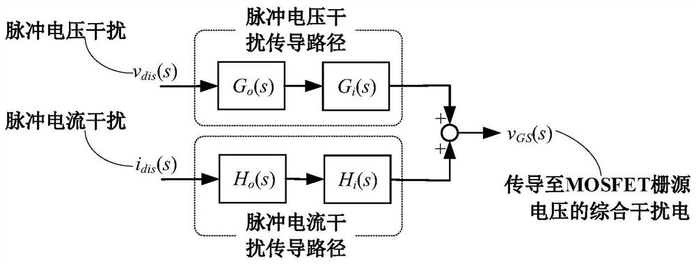
[0054] figure 1 It is a transfer function block diagram of a MOSFET gate-source voltage interference conduction path model described in the present invention. Such as figure 1 As shown, the model includes the following:

[0055] (1) Both the pulse voltage interference conduction path and the pulse current interference conduction path are described.

[0056] (2) The model includes a double-loop transfer function desc...


PUM


Abstract

The invention provides an MOSFET gate-source voltage interference conduction path model. The MOSFET gate-source voltage interference conduction path model comprises a double-loop transfer function fordescribing a pulse voltage and pulse current interference conduction process and a characteristic equation for describing a standard second-order system of an interference conduction path. The modelis used for revealing a gate-source voltage interference mechanism occurring when a high-frequency high-power converter and an MOSFET are turned on and turned off at a high speed, and the interferenceconduction path model can comprehensively consider the influence of pulse voltage and pulse current on MOSFET gate-source voltage interference and is used for visually and rapidly judging the rationality of the MOSFET driving parameters, an MOSFET packaging structure and the PCB layout designin in a power conversion system .

Description

technical field [0001] The invention relates to a MOSFET gate-source voltage interference conduction path model. Background technique [0002] In general, the working voltage of SiC MOSFET (about kV level) is much higher than the working current (about A level) in value. Therefore, the pulse voltage is the main interference source of gate-source voltage interference, although in terms of value, considering the pulse voltage The mathematical analysis of interference has good accuracy within the allowable range of error, but under the premise of studying the package difference and the interference caused by the driving resistance to the gate-source voltage, the interference of the pulse current cannot be ignored. The interference of the pulse current on the gate-source voltage can be roughly divided into two categories: the first type, the distributed voltage interference is induced in the drive circuit through the change of the space electromagnetic field, which belongs to th...

Claims


Application Information

Patent Timeline
Patent Type & Authority Applications(China)
IPC IPC(8): G06F30/20G06F30/30G06F17/15
CPCG06F17/15G06F30/20G06F30/30
Inventor 邵天骢郑琼林李志君李虹黄波邱志东张志朋王作兴王佳信
Owner BEIJING JIAOTONG UNIV
Why Eureka
Try Eureka