Electrostatic chuck system and semiconductor processing equipment
An electrostatic chuck and electrostatic technology, applied in the manufacture of semiconductor/solid-state devices, circuits, discharge tubes, etc., can solve the problems of poor etching uniformity, uniform formation, and difficulty in ensuring the uniformity of adhesive thickness, so as to improve uniformity sexual effect
- Summary
- Abstract
- Description
- Claims
- Application Information
AI Technical Summary
Problems solved by technology
Method used
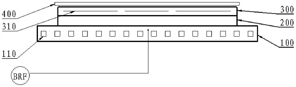
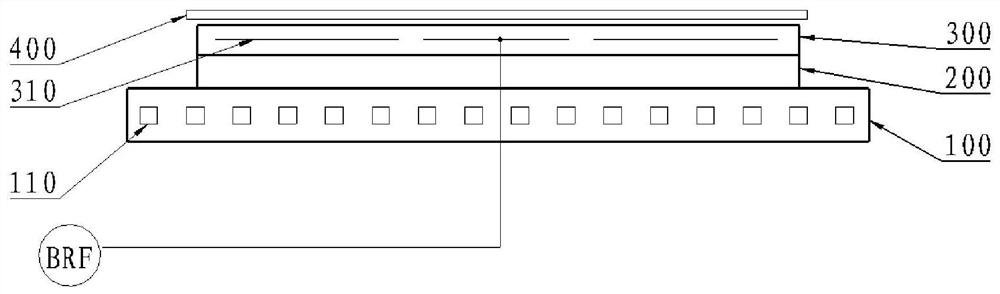
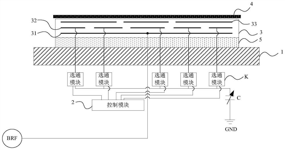
Image

Examples
Embodiment Construction
[0029] Specific embodiments of the present invention will be described in detail below in conjunction with the accompanying drawings. It should be understood that the specific embodiments described here are only used to illustrate and explain the present invention, and are not intended to limit the present invention.
[0030] Unless otherwise defined, the technical terms or scientific terms used in the embodiments of the present invention shall have the usual meanings understood by those skilled in the field of the present invention. "First", "second" and similar words used in the present invention do not indicate any order, quantity or importance, but are only used to distinguish different components. Likewise, "comprising" or "comprises" and similar words mean that the elements or items appearing before the word include the elements or items listed after the word and their equivalents, and do not exclude other elements or items. Words such as "connected" or "connected" are ...
PUM
| Property | Measurement | Unit |
|---|---|---|
| Thickness | aaaaa | aaaaa |
| Diameter | aaaaa | aaaaa |
Abstract
Description
Claims
Application Information
 - R&D
- Intellectual Property
- Life Sciences
- Materials
- Tech Scout
- Unparalleled Data Quality
- Higher Quality Content
- 60% Fewer Hallucinations
Browse by: Latest US Patents, China's latest patents, Technical Efficacy Thesaurus, Application Domain, Technology Topic, Popular Technical Reports.
© 2025 PatSnap. All rights reserved.Legal|Privacy policy|Modern Slavery Act Transparency Statement|Sitemap|About US| Contact US: help@patsnap.com