PCB electroplating method and PCB electroplating equipment

A technology for PCB boards and electroplating equipment, which is applied in the field of PCB board electroplating methods and PCB board electroplating equipment, and can solve the problems of poor flow penetration and depth capabilities of liquid chemicals

Active Publication Date: 2021-03-16
深圳明阳芯蕊半导体有限公司
View PDF9 Cites 2 Cited by
  • Summary
  • Abstract
  • Description
  • Claims
  • Application Information

AI Technical Summary

Problems solved by technology

[0004] see image 3 , in the electroplating process, because the PCB board 2 to be plated in the middle is in the spraying center of the nozzle 1 (specifically, the nozzles distributed on it), the process of the chemical liquid penetrating into the hole, even if the staggering of the nozzles or the alignment of the nozzles is changed Staggered, there is always one-sided interference and double-sided interference generated by the nozzle jet in the liquid, resulting in poor penetration and depth capabilities of the liquid medicine flow

Method used


Image

  • PCB electroplating method and PCB electroplating equipment
  • PCB electroplating method and PCB electroplating equipment
  • PCB electroplating method and PCB electroplating equipment

Examples


Embodiment approach

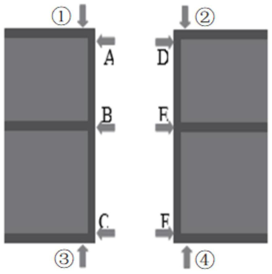
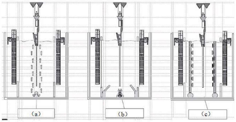
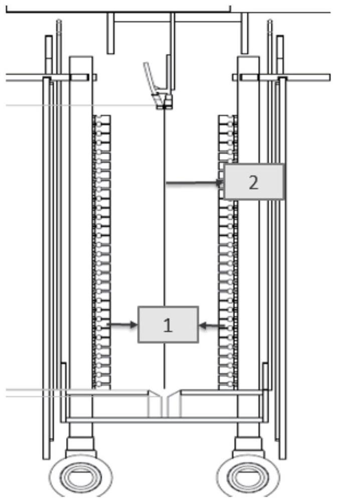
[0034] In an alternative embodiment, the present invention provides a PCB board electroplating method, which includes the following steps: S1: Fix the PCB board in the electroplating tank body of the electroplating equipment, wherein, set the electroplating tank body in the electroplating equipment There is a fixing assembly for fixing the PCB board, and a first nozzle group and a second nozzle group are respectively provided on both sides of the PCB board; S2: controlling part of the nozzles of the first nozzle group to perform the liquid medicine ejection operation, and Control the corresponding part of the nozzles of the second nozzle group to perform the liquid medicine suction operation; at the same time control the rest of the nozzles of the first nozzle group to perform the liquid medicine suction operation, and control the corresponding remaining nozzles of the second nozzle group Part of the nozzles perform the liquid medicine spraying operation, so that a positive pre...


PUM


Abstract

The invention provides a PCB electroplating method and PCB electroplating equipment. The PCB electroplating method comprises the steps of S1, fixing a PCB in an electroplating tank body of the electroplating equipment, wherein a fixing assembly for fixing the PCB is arranged in the electroplating tank body of the electroplating equipment, and a first nozzle set and a second nozzle set are correspondingly arranged at the two sides of the PCB; and S2, controlling the first nozzle set and the second nozzle set to alternately execute a chemical liquid spraying operation and a chemical liquid suction operation, so that a positive pressure difference and a negative pressure difference are formed on the two sides of the PCB in the chemical liquid spraying process. According to the PCB electroplating method and the PCB electroplating equipment, the penetrability of chemical liquid flowing in holes during side spraying is improved, the good deep plating capacity is achieved, and the breakthrough that the TP value of the thickness-diameter ratio of 40: 1 is 100% can be achieved.

Description

technical field [0001] The invention relates to the technical field of circuit boards, in particular to a PCB board electroplating method and PCB board electroplating equipment. Background technique [0002] In the PCB design in recent years, thick and large boards and small drilling apertures have gradually formed a trend. In the field of plated through holes, the ratio of board thickness to aperture has increased from 10:1 to 40:1 (hereinafter referred to as the thickness-to-diameter ratio), which is To ensure that the copper plating thickness in the small hole meets the minimum thickness required by the customer, we have the probability of proposing the minimum deep plating capacity TP value (Through power for short) in the hole in order to test the distribution ability in the hole produced by the electroplating copper bath with the potion: Inspection standards such as figure 1 Shown: Minimum TP value = AVG(B+E) / AVG(①+②+③+④). 6 points of copper thickness in the hole-A, ...

Claims


Application Information

Patent Timeline
Patent Type & Authority Applications(China)
IPC IPC(8): C25D5/08C25D7/00C25D17/00H05K3/18
CPCC25D5/08C25D7/00C25D17/00H05K3/188
Inventor 吴勇军
Owner 深圳明阳芯蕊半导体有限公司
Why Eureka
Try Eureka