Three-dimensional imaging device and method based on optical frequency comb interferometry

An optical frequency comb and three-dimensional imaging technology, applied in the direction of measuring devices, radio wave measuring systems, electromagnetic wave re-radiation, etc., can solve the problems of destroying samples, low measurement accuracy, and complicated measurement systems, and achieve real-time online imaging and measurement High precision, beneficial to equipment integration

Active Publication Date: 2021-03-19
SHANXI UNIV
View PDF9 Cites 6 Cited by
  • Summary
  • Abstract
  • Description
  • Claims
  • Application Information

AI Technical Summary

Problems solved by technology

Photogrammetry is the earliest material characterization method proposed. This method can capture the measured sample in a wide range and properly process the sample photos. However, in order to realize the three-dimensional imaging of the sample, two or more cameras are needed. Not only complicate the mea

Method used


Image

  • Three-dimensional imaging device and method based on optical frequency comb interferometry
  • Three-dimensional imaging device and method based on optical frequency comb interferometry
  • Three-dimensional imaging device and method based on optical frequency comb interferometry

Examples


Embodiment Construction

[0025] In order to make the purpose, technical solutions and advantages of the embodiments of the present invention clearer, the technical solutions in the embodiments of the present invention will be clearly and completely described below. Obviously, the described embodiments are part of the embodiments of the present invention, rather than All the embodiments; based on the embodiments of the present invention, all other embodiments obtained by persons of ordinary skill in the art without making creative efforts all belong to the protection scope of the present invention.

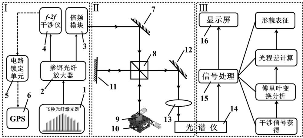
[0026] Such as figure 1 As shown, the embodiment of the present invention provides a three-dimensional imaging device based on optical frequency comb interferometry, including a light source system I, an interferometry system II and a signal processing system III. Wherein, the light source system 1 includes a femtosecond fiber laser 1, an erbium-doped fiber amplifier 2, a frequency doubling module 3, f -...


PUM

PropertyMeasurementUnit
Wavelength rangeaaaaaaaaaa

Abstract

The invention belongs to the technical field of material morphology characterization, and particularly relates to a device and a method capable of performing three-dimensional imaging on a solid material. The device comprises a light source system, a light splitting element, a two-dimensional translation stage, a first reflector, a spectrograph and a signal processing system, the light source system comprises a femtosecond fiber laser, and the repetition frequency and the offset frequency of the femtosecond fiber laser are locked to an atomic clock to form an optical frequency comb; after a light beam emitted by the light source system is divided into two beams by the light splitting element, one beam is used as a reference light beam and vertically enters the first reflector; one beam isused as a detection light beam to be incident to the surface of a to-be-detected sample placed on the two-dimensional platform; the reference light beam and the detection light beam are respectively reflected and then returned to the light splitting element, the reference light beam and the detection light beam coincide at the light splitting element and interfere, and interference signals enter the spectrograph and then are calculated by the signal processing system to obtain the three-dimensional morphology of the to-be-detected sample. The three-dimensional morphology imaging of the sampleto be detected is realized, the measurement precision is high, and the device can be widely applied to the field of materials.

Description

technical field [0001] The invention belongs to the technical field of material morphology characterization, and in particular relates to a device and method capable of performing three-dimensional imaging on solid materials. Background technique [0002] Optical frequency combs appear as optical frequency sequences with equal frequency intervals in the frequency domain, and as electromagnetic field oscillation envelopes with femtosecond time width in the time domain. The time width satisfies the Fourier transform relationship. The distribution characteristics of ultrashort pulses in the time domain and frequency domain are similar to the combs we use every day. They are visually called frequency combs in the optical band, or "optical combs" for short. The optical comb is equivalent to an optical frequency synthesis generator. It is the most effective tool for absolute optical frequency measurement so far. It can accurately and simply link the atomic microwave frequency stan...

Claims


Application Information

Patent Timeline
IPC IPC(8): G01S17/89G01S7/48
CPCG01S17/89G01S7/4808
Inventor 元晋鹏汪丽蓉王三丹
Owner SHANXI UNIV
Why Eureka
Try Eureka