Double-layer PCB welding device, clamp and method and welding clamp for PCB and connecting pin

A technology of welding fixtures and connecting pins, which is applied in the direction of welding/welding/cutting objects, auxiliary devices, welding equipment, etc., which can solve the problems of electronic components that cannot be placed down, large size of connecting pins, and occupying too much space, etc., to achieve positioning The effect of high fixing accuracy, consistent quality, and easy operation

Active Publication Date: 2021-03-26
LINKTEL TECH CO LTD
View PDF7 Cites 3 Cited by
  • Summary
  • Abstract
  • Description
  • Claims
  • Application Information

AI Technical Summary

Problems solved by technology

[0003] In the field of optical modules, there are agreements to limit the size of the structure. Modules that need to meet certain specific performance will need to use double-layer PCB (Printed Circuit Board, printed circuit board) ) structure, the existing chips occupy close to the ultimate space on the PCB. The conventional manufacturing process is to use soft tape welding, or add connectors and connect with soft tape, which will increase the occupied space on the PCB, resulting in The electronic components on the PCB cannot be placed down. On the one hand, there is a problem of space occupation; instead of using the soft belt connection method, the connection pin headers with plastic parts in the middle of the batch on the market are used, because the connection pin headers on the market are larger in size. Still take up too much space to borrow
If you use 3D printing to customize, it is difficult to achieve the accuracy when printing with ordinary machines and materials, and the price is too high when using special materials

Method used


Image

  • Double-layer PCB welding device, clamp and method and welding clamp for PCB and connecting pin
  • Double-layer PCB welding device, clamp and method and welding clamp for PCB and connecting pin
  • Double-layer PCB welding device, clamp and method and welding clamp for PCB and connecting pin

Examples


Embodiment 1

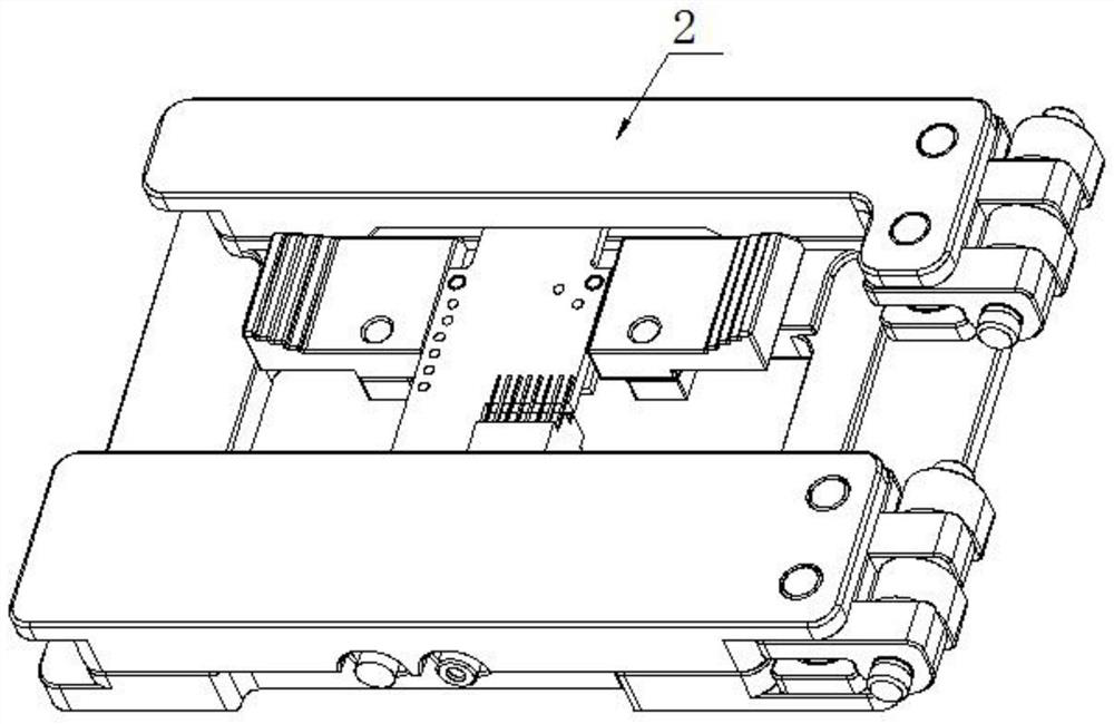
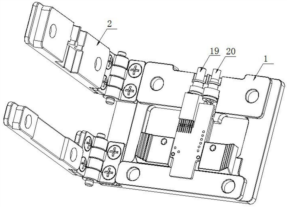
[0036] see Figure 1 to Figure 7 , the embodiment of the present invention provides a double-layer PCB welding fixture, including a first base 1, the first sub-board limiting structure and the main board limiting structure are installed on the first base 1, the sub-board is positioned on the first sub-board On the limit structure of the plate, the connecting pin 5 is welded and fixed on the secondary plate 3, the main plate 4 is positioned on the limit structure of the main plate, the main plate is located above the secondary plate, the main plate and the secondary plate are parallel, and there is a gap between the main plate and the secondary plate. The connecting pins on the sub-board pass through the reserved connecting holes on the main board. The main board and the auxiliary board are horizontally supported on the first base 1 .

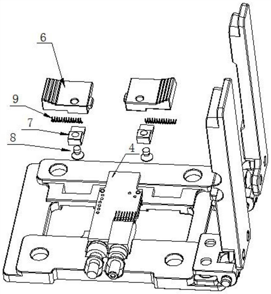
[0037] Further, the first sub-board limiting structure includes two sliders 6, the sliders 6 are arranged on the first base 1 without falling ...

Embodiment 2

[0047] see Figure 8 and Figure 9 , this embodiment discloses a welding fixture for PCB and connection pins, including a second base 14, at least one clamping station is arranged on the second base 14, and each clamping station of the second base 14 The upper support has at least two sub-boards overlapping up and down. The top sub-board of each clamping station is a sub-board 16 with electronic components, and the rest of the sub-boards of each clamping station do not contain electronic components. The sub-board 17 of the device, the connection holes reserved for each layer of sub-boards of each clamping station correspond to each other, and the connecting pins are inserted into the connection holes reserved for each layer of sub-boards in sequence from top to bottom, and the second Each clamping station of the base 14 is provided with a second sub-board limiting structure for limiting the position of each sub-board. The connection pins of this embodiment are inserted into ...

Embodiment 3

[0053] see Figure 1 to Figure 9 , the invention discloses a double-layer PCB welding device, including the welding jig for PCB and connecting pins described in the second embodiment and the welding jig for the double-layer PCB described in the first embodiment.


PUM


Abstract

The invention relates to a double-layer PCB welding device, clamp and method and a welding clamp for a PCB and a connecting pin. The double-layer PCB welding device comprises the welding clamp for thePCB and connecting pin and the double-layer PCB welding clamp, wherein the connecting pin is welded and fixed to an auxiliary plate through the welding clamp for the PCB and connecting pin, two sliding blocks of the double-layer PCB welding clamp are pushed aside, then the auxiliary plate is placed on the lower layer of the clamp, a main plate is placed in the upper layer of the clamp through limiting and clamping of the sliding blocks, the clamp is provided with a limiting protrusion, the limiting protrusion is matched with pressing of a first cover plate for fixation, then welding is conducted, and therefore two welded plates are parallel, and high-precision welding and positioning of the connecting pin are achieved. According to the double-layer PCB welding device, clamp and method andthe welding clamp for the PCB and the connecting pin, the structural design is reasonable, use and operation are easy and convenient, the positioning and fixing precision is high, the cost is low, the implementation time is short, and the double-layer PCB welding device, clamp and method and the welding clamp for the PCB and the connecting pin are capable of being applied to the connecting, welding and assembling process of double-layer PCBs of the same size, in the same space and of different types.

Description

technical field [0001] The invention belongs to the field of optical module design and manufacture, and in particular relates to a double-layer PCB welding device, fixture and method, and a welding fixture for PCB and connecting pins. Background technique [0002] Communication equipment has higher and higher requirements for small size and high interface density. On the one hand, it must be able to achieve performance, on the one hand, it must be able to meet the requirements of use, and on the other hand, it must be able to effectively meet the requirements of passing tests. Module integration is getting higher and higher, and the space is getting more and more compact. Under the existing structural space constraints, to achieve a high degree of integration requires maximizing space utilization. [0003] In the field of optical modules, there is an agreement to limit the size of the structure. Modules that need to meet certain specific performance will need to use a double...

Claims


Application Information

Patent Timeline
Patent Type & Authority Applications(China)
IPC IPC(8): B23K37/04B23K37/00B23K101/36
CPCB23K37/0443B23K37/00B23K2101/42
Inventor 汤慧敏彭峰李林科吴天书杨现文张健
Owner LINKTEL TECH CO LTD
Why Eureka
Try Eureka