One-dimensional nanometer electrode material, and preparation method and application thereof

A technology of nano-electrodes and silicon nano-wire arrays, which is applied in the direction of material analysis, nanotechnology, and material analysis through electromagnetic means, can solve problems such as excessive high voltage, and achieve the effect of reducing operating voltage and low breakdown voltage

Inactive Publication Date: 2013-08-21
NANTONG UNIVERSITY
View PDF5 Cites 10 Cited by
  • Summary
  • Abstract
  • Description
  • Claims
  • Application Information

AI Technical Summary

Problems solved by technology

Although this operating voltage is much lower than the thousands of volts of conventio

Method used


Image

  • One-dimensional nanometer electrode material, and preparation method and application thereof
  • One-dimensional nanometer electrode material, and preparation method and application thereof
  • One-dimensional nanometer electrode material, and preparation method and application thereof

Examples


Embodiment Construction

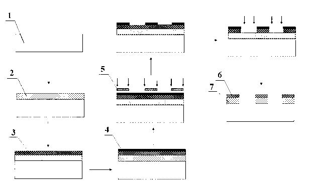
[0029] The present invention will be described in detail below in conjunction with the accompanying drawings.

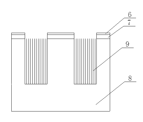
[0030] Such as figure 1 As shown, the one-dimensional nanometer electrode material of the present invention includes a silicon wafer substrate 8 , a silicon dioxide film 7 and a silicon nitride film 6 , and a silicon nanowire array 9 . The silicon dioxide film 7 and the silicon nitride film 6 are rectangular, and have the same size and shape (the silicon dioxide film 7 and the silicon nitride film 6 can be of various shapes, and the regular shape is preferable to facilitate mask preparation). The silicon dioxide film 7 is evenly distributed on the surface of the silicon wafer substrate 8 at intervals. The silicon nitride film 6 is deposited on the corresponding surface of the silicon dioxide film. The surface of the silicon wafer substrate between the silicon dioxide films 7 is etched to form a silicon nanowire array 9 . The silicon dioxide film 7 has a thickness ...


PUM

PropertyMeasurementUnit
Total thicknessaaaaaaaaaa
Thicknessaaaaaaaaaa
Thicknessaaaaaaaaaa

Abstract

The invention discloses a one-dimensional nanometer electrode material, and a preparation method and an application thereof. The one-dimensional nanometer electrode material comprises a silicon slice substrate, and a silicon nanowire array which stands on the silicon slice substrate, and also comprises silicon dioxide films and silicon nitride films; the silicon dioxide films are respectively coated at two ends of the surface of the silicon slice substrate; the silicon nitride films are deposited on the surfaces of corresponding silicon nitride films; the surface of the silicon slice substrate, which is not covered by the silicon dioxide films, forms the silicon nanowire array in an etching manner; and the total thicknesses of the silicon dioxide films and the silicon nitride films are 0.5-10 microns. An ionization structure built by the preparation method is low in ionization breakdown voltage in air, and is suitable for use of a daily portable apparatus.

Description

technical field [0001] The invention relates to a one-dimensional nanometer electrode material, in particular to a one-dimensional nanometer electrode material with an ionized structure with tiny gaps. Background technique [0002] Conventional gas sensors are divided into two categories, one based on gas adsorption and the other based on gas ionization. The adsorption and desorption of gas will not only affect the response time, but also affect the durability. With the development of nanotechnology, the ionization of gas molecules has the function similar to fingerprint identification, but the ultra-high working voltage is not suitable for general application. The miniaturized gas ionization sensor provides a solution for reducing the operating voltage. [0003] When working at normal temperature and pressure, each gas has a different breakdown electric field. In a uniform electric field, the voltage required to cause gas ionization is usually on the order of hundred...

Claims


Application Information

Patent Timeline
IPC IPC(8): G01N27/68B82Y30/00B82Y15/00
Inventor 陈云尹海宏宋长青黄静朱海峰施敏张振娟
Owner NANTONG UNIVERSITY
Why Eureka
Try Eureka