Military FPGA universal reconstruction circuit based on JTAG interface

A technology for reconstructing circuits and interfaces, applied in the design program of CPLD and FPGA field, can solve problems such as unfavorable on-site debugging, affecting the miniaturization of board-level products, and large interface area.

Pending Publication Date: 2021-04-02
BEIJING MXTRONICS CORP +1
View PDF0 Cites 2 Cited by
  • Summary
  • Abstract
  • Description
  • Claims
  • Application Information

AI Technical Summary

Problems solved by technology

[0002] In current weapons and equipment, SRAM-type FPGA and CPLD are widely used. At present, the mainstream manufacturers of SRAM-type FPGA and CPLD are Xilinx and Altera. In the actual board-level product design, if products from both manufacturers are included, then It is often impossible to put it in the same JTAG daisy chain for debugging and programming, which affects the mi

Method used


Image

  • Military FPGA universal reconstruction circuit based on JTAG interface
  • Military FPGA universal reconstruction circuit based on JTAG interface
  • Military FPGA universal reconstruction circuit based on JTAG interface

Examples


Embodiment 1

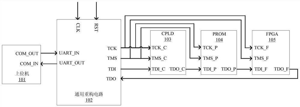
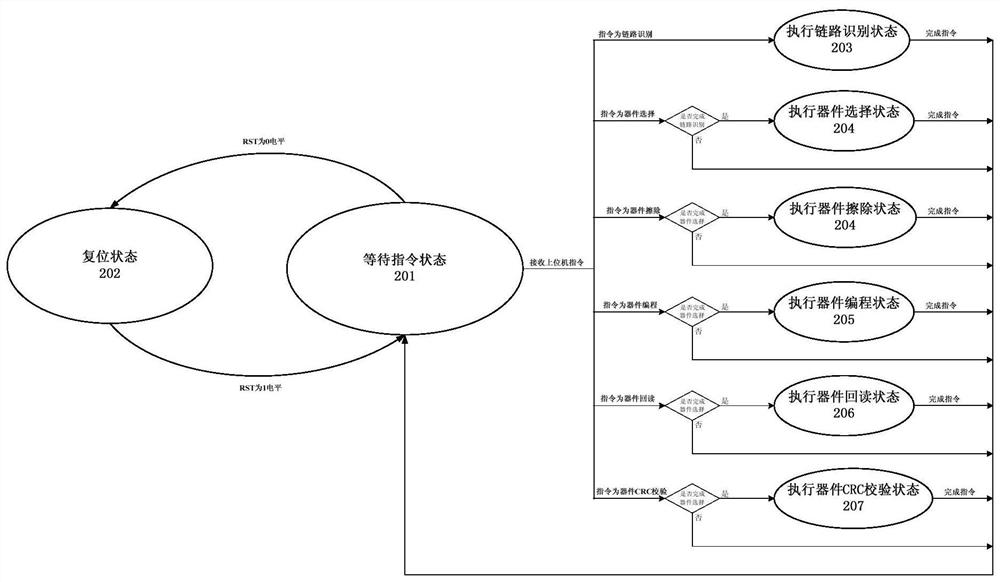
[0124] like image 3 and Figure 4Shown is the implementation flow chart of the reconfiguration circuit of the present invention. The reconfiguration circuit 102 of the present invention includes five working states, including the waiting instruction state 201, the reset state 202, the execution "link identification" state 203, and the execution "device selection" state 204. 1. Execute the "device erasing" state 205, execute the "device programming" state 206, execute the "device readback" state 207, execute the "device CRC check" state 208, the implementation method of the reconfiguration circuit 102 of the present invention is realized by a state machine , the specific implementation process is as follows:

[0125] Step (1), the initial state of the reconfiguration circuit 102 after power-on is a state of waiting for an instruction. In the state of waiting for an instruction, if the RST signal input from the outside through the RST pin is "0" level, it will enter the reset ...

Embodiment 2

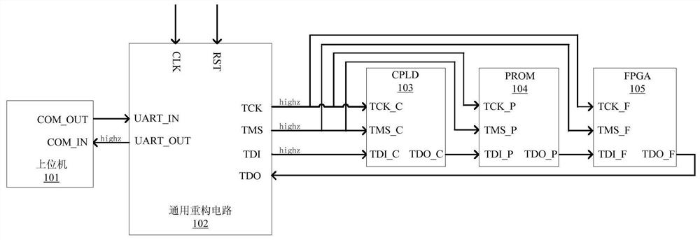
[0134] After power-on, connect the RST pin of the reconfiguration circuit 102 to “0” level, then the reconfiguration circuit 102 suspends its work and enters the reset state 202 . In the reset state, the reconfiguration circuit clears all internal registers, and at the same time outputs the TCK pin, TMS pin, TDI pin, and UART_OUT pin to a high-impedance state. At this time, the reconstruction circuit 102 does not respond to the instructions of the host computer 101 .

Embodiment 3

[0136] After power-on, connect the CLK pin of the reconfiguration circuit 102 to a clock signal with a fixed frequency of 40 MHz, and connect the RST pin to "0" level, and the reconfiguration circuit 102 enters the reset state 202, clears all internal registers, and outputs the Pin high impedance, RST pin is connected to "1" level, the reconstruction circuit enters the waiting command state 201, and starts to receive the command information of the host computer 101 through the UART_IN pin. There are 6 commands of the host computer, which are link identification, Device selection, device erasing, device programming, device readback, device CRC check, the reconfiguration circuit enters the specified state according to the instruction information.

[0137] The instruction received by the reconfiguration circuit for the first time only responds to the "link identification" instruction, and enters the execution link identification state 203. The reconfiguration circuit 102 sends a r...


PUM


Abstract

The invention relates to a military FPGA universal reconstruction circuit based on a JTAG interface, and the reconstruction circuit is provided with four input pins and four output pins, can be connected with pins of an FPGA, a CPLD and a PROM, receives an instruction of an upper computer, carries out the backward reading IDCODE operation of the FPGA, the CPLD and the PROM in a link through the JTAG interface, determines the model of a device, and according to an instruction of the upper computer, capable of erasing, programming, reading back and checking the selected device through the JTAG interface; by means of the reconstruction circuit, the purpose of designing FPGA and CPLD design programs in an on-site change system after product installation is achieved, external interfaces of products are effectively reduced, the distance of debugging cables is prolonged, and the on-site debugging efficiency of installed products is improved.

Description

technical field [0001] The invention relates to a military FPGA general reconfiguration circuit based on a JTAG interface and an implementation method thereof, in particular to a design program for FPGA and CPLD in an on-site remote change system after product installation, and belongs to the technical field of integrated circuits. Background technique [0002] In current weapons and equipment, SRAM-type FPGA and CPLD are widely used. At present, the mainstream manufacturers of SRAM-type FPGA and CPLD are Xilinx and Altera. In the actual board-level product design, if products from both manufacturers are included, then It is often impossible to put it in the same JTAG daisy chain for debugging and programming, which affects the miniaturization of board-level products; [0003] At the same time, during the field test of installed products, the JTAG interface is usually used to program and change the design program. The disadvantages are that the interface occupies a large are...

Claims


Application Information

Patent Timeline
IPC IPC(8): G06F8/61
CPCG06F8/61
Inventor 陈雷孙华波李政李学武张帆李琦李明哲
Owner BEIJING MXTRONICS CORP
Why Eureka
Try Eureka