Self-luminous display panel

A display panel, self-luminous technology, applied in the direction of organic semiconductor devices, electrical components, diodes, etc., can solve the problem of difficulty in fully reducing chromaticity changes, and achieve the effect of refinement, reduction of chromaticity changes, and high precision

Pending Publication Date: 2021-04-09
JOLED INC
View PDF4 Cites 0 Cited by
  • Summary
  • Abstract
  • Description
  • Claims
  • Application Information

AI Technical Summary

Problems solved by technology

[0008] However, in the structure described in Patent Document 1, there is a technical problem that it is difficult to sufficiently reduce the change in chromaticity when viewed from an oblique direction in a high-definition organic EL display panel.

Method used


Image

  • Self-luminous display panel
  • Self-luminous display panel
  • Self-luminous display panel

Examples


Deformed example 1

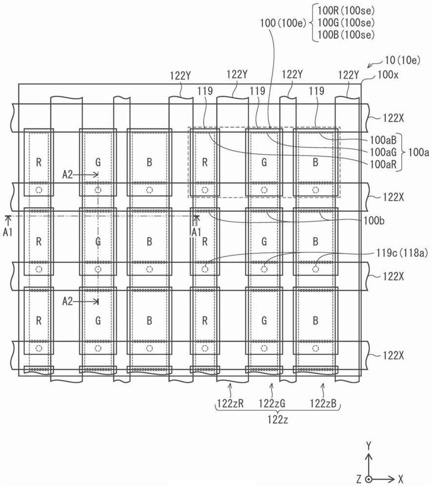
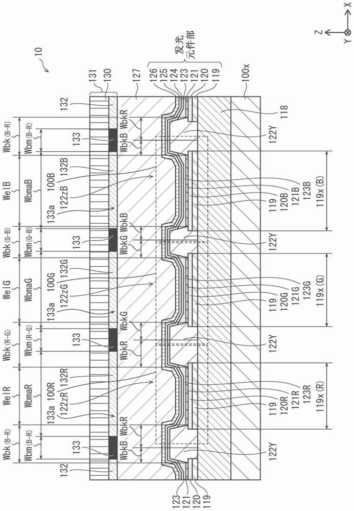
[0250] In the display panel 10 according to the embodiment, the row widths Wbma(R-G), Wbma(G-B), and Wbma(B-R) of the openings 133a in the light-shielding film 133 are related to the light emission of the light-emitting element 100 . Regardless of the color, the row direction width Wbm(R-G), Wbm(G-B), Wbm(B-R) of the gate part between the openings 133a is also independent of the light-emitting color of the light-emitting element 100, etc. price composition. In the display panel 10A according to Modification 1, the widths Wbm(R-G), Wbm(G-B), and Wbm(B-R) in the row direction of the portion configured as the gate between the openings 133 a are also determined by the light-emitting element 100 As a result, the row-wise widths Wbma(R-G), Wbma(G-B), and Wbma(B-R) of the openings 133a in the light-shielding film 133 differ depending on the light-emitting color of the light-emitting element 100, This point is different from the embodiment.

[0251] Figure 14 is the display panel ...

Deformed example 2

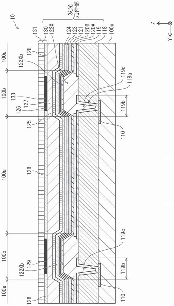
[0254] In the display panel 10 according to the embodiment, as an example, the maximum distance in the emission direction between the light emission reference point of the light emitting element 100B and the edge of the opening 133a of the light shielding film 133 is used as compared with the light emitting elements 100R and G. LB explains the implementation in a longer way. In this embodiment, as described above, the lengths 119 x (B), (G), and (R) in the row direction of the pixel electrodes 119 in the light-emitting elements 100B, 100G, and 100R are configured in the order of the light-emitting elements 100B, 100G, and 100R. From large to small, the light-shielding rate of the light-emitting element 100B is the smallest. On the other hand, by adopting the above structure in the display panel 10, the light-shielding ratio of the light-emitting element 100 whose pixel electrode 119 has the largest length in the row direction is increased, thereby effectively compensating for ...


PUM

PropertyMeasurementUnit
thicknessaaaaaaaaaa
reflectanceaaaaaaaaaa

Abstract

A self-luminous display panel having a structure capable of improving definition and reducing chromaticity changes in emitted light when a display image is viewed from an oblique direction, the self-luminous display panel is provided with: a plurality of light-emitting elements (100) that emit light having different colors for each sub-pixel (100se) constituting a pixel; a plurality of column cofferdams (122Y) which are arranged between the light-emitting elements (100) in the row direction and extend in the column direction; and a light-shielding film (133) that is provided on the downstream side of the light-emitting elements (100) in the emission direction and that has openings (133a) provided at positions facing the light-emitting elements (100) in plan view. The distance between the edge of the opening (133a) of the light-shielding film (133) in the row direction and the light-emitting element (100) varies depending on the light-emitting color of the light-emitting element (100) by varying the width of a portion of the column cofferdam (122Y) adjacent to the light-emitting element (100) in the row direction, said portion being located on the light-emitting element (100) side.

Description

technical field [0001] The present disclosure relates to a display panel in which pixels including light-emitting elements such as organic electroluminescence elements (hereinafter referred to as "organic EL elements") are two-dimensionally arranged along a main surface of a substrate, and a method for manufacturing the display panel. Background technique [0002] In recent years, organic EL display panels in which a plurality of organic EL elements are arranged in a matrix on a substrate have been put into practical use as display panels used in display devices such as digital televisions. An organic EL element has a basic structure in which a light-emitting layer containing an organic light-emitting material is disposed between a pair of electrodes. When driven, a voltage is applied between the pair of electrodes, and light is emitted by recombination of holes and electrons injected into the light-emitting layer. [0003] A top-emission organic EL element has an element st...

Claims


Application Information

Patent Timeline
Patent Type & Authority Applications(China)
IPC IPC(8): H01L27/32H01L51/52
CPCH10K59/35H10K59/126H10K59/122H10K50/85H10K59/352H10K59/38H10K50/865H10K2102/3026H10K71/00H10K50/852
Inventor 福冈健太
Owner JOLED INC
Why Eureka
Try Eureka