Automatic mass production type clamp for microelectronic device packaging

A microelectronic device and mass production technology, which is applied in the direction of electrical components, semiconductor/solid-state device manufacturing, circuits, etc., can solve problems such as poor production efficiency and low efficiency, and achieve improved production efficiency, firm product fixation, and increased vacuum adsorption strength Effect

Pending Publication Date: 2021-04-13
INNOGRATION SUZHOU
View PDF0 Cites 0 Cited by
  • Summary
  • Abstract
  • Description
  • Claims
  • Application Information

AI Technical Summary

Problems solved by technology

[0005] In view of the technical problems caused by frequent replacement of fixtures and low production efficiency in the above-mentioned production process, the purpose of the present invention is to provide an automatic mass-production fixture for microelectronic device packaging, so that there is no need to replace the fixture during the packaging process, and the product is fixed Firm, greatly improving production efficiency

Method used


Image

  • Automatic mass production type clamp for microelectronic device packaging
  • Automatic mass production type clamp for microelectronic device packaging
  • Automatic mass production type clamp for microelectronic device packaging

Examples


Embodiment

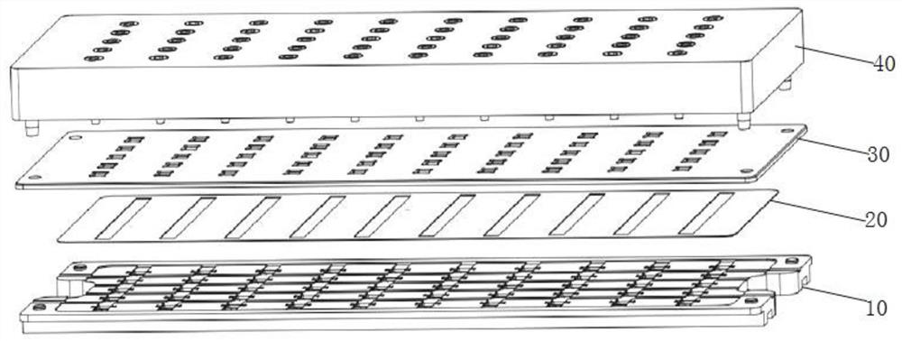
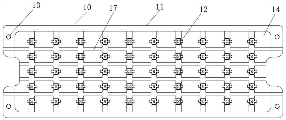
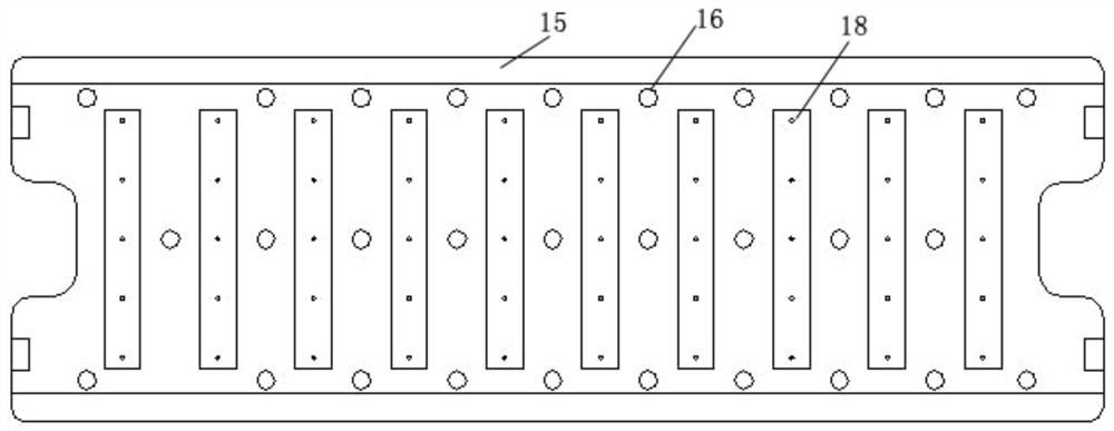
[0033] Such as figure 1 As shown, an automatic mass-production jig for microelectronic device packaging includes a carrier layer 10, a cover layer 20, a guide layer 30, and a pressing layer 40 that are placed in sequence from bottom to top, and are placed on the carrier layer 10. Put the corresponding product, and then add the cover layer 20, such a combination can be transported on the machine, and the product is firmly fixed and will not fall out; after the chip placement or bonding and wiring operations are completed , add the guide plate layer 30 in sequence on the above combination, then place the cover of the product to be operated, and finally cover the pressing plate layer 40, and then it can be put into the oven for sealing and curing.

[0034] Preferably, the thickness of the pressing plate layer 40 is greater than that of the carrier plate layer 10 , greater than that of the guide plate layer 30 , and greater than that of the cover plate layer 20 .

[0035] Such as...


PUM


Abstract

The invention discloses an automatic mass production type clamp for microelectronic device packaging, which comprises a carrier plate layer, a cover plate layer, a guide plate layer and a pressing plate layer sequentially arranged from bottom to top, wherein a plurality of product positioning grooves and a first positioning structure are arranged on the upper surface of the carrier plate layer, the cover plate layer covers the product positioning grooves, a window is formed in the position, corresponding to the product positioning groove, of the cover plate layer, the guide plate layer is provided with a second positioning structure matched with the first positioning structure, a cover positioning groove is formed in the upper surface of the guide plate layer, and the center of the cover positioning groove coincides with the center of the product positioning groove. The pressing plate layer is provided with a third positioning structure matched with the second positioning structure, and a protruding part is arranged at the position, corresponding to the cover positioning groove, of the lower surface of the pressing plate layer. Therefore, the clamp does not need to be replaced in the packaging process, the product is firmly fixed, and the production efficiency is greatly improved.

Description

technical field [0001] The invention relates to an automatic mass production carrier, in particular to an automatic mass production jig for microelectronic device packaging. Background technique [0002] The packaging form of microelectronic devices refers to the housing used to install semiconductor integrated circuit chips. It not only plays the role of installing, fixing, sealing, protecting the chip and enhancing the electrothermal performance, but also connects the contacts on the chip to the pins of the package shell with wires, and these pins pass through the wires on the printed circuit board. Connect with other devices to realize the connection between the internal chip and the external circuit. Because the chip must be isolated from the outside world to prevent impurities in the air from corroding the chip circuit and causing electrical performance degradation. [0003] The mass production of existing microelectronic device packaging uses a set of fixtures for th...

Claims


Application Information

Patent Timeline
IPC IPC(8): H01L21/687H01L21/68
CPCH01L21/68785H01L21/68
Inventor 刘长春
Owner INNOGRATION SUZHOU
Why Eureka
Try Eureka