
Gold finger circuit board processing method and gold finger circuit board

A processing method and gold finger technology, which is applied in printed circuit, printed circuit manufacturing, multi-layer circuit manufacturing, etc., can solve problems such as gold finger failure, collision or scratching, and affecting gold finger processing, so as to improve processing quality and reduce possible Sexuality and the effect of prolonging the service life

Active Publication Date: 2022-06-17
HUAIAN TECHUANG TECH CO LTD
View PDF9 Cites 0 Cited by
  • Summary
  • Abstract
  • Description
  • Claims
  • Application Information

AI Technical Summary

Problems solved by technology

Since the gold finger is directly exposed to the outside, during processing, the processing equipment or human hands are likely to directly touch the contact piece of the gold finger, resulting in damage to the surface of the gold finger contact piece, which in turn affects the processing of the gold finger
In addition, in daily use, the contact sheet is easy to collide or scratch with external objects, causing the contact sheet of the gold finger to be easily damaged, which in turn affects the information transmission efficiency and even causes the gold finger to fail. Therefore, the traditional multi-layer circuit board gold finger Processing methods Traditional circuit board gold fingers often have a short service life

Method used


Image

  • Gold finger circuit board processing method and gold finger circuit board
  • Gold finger circuit board processing method and gold finger circuit board
  • Gold finger circuit board processing method and gold finger circuit board

Examples


Embodiment Construction

[0036] In order to facilitate understanding of the present invention, the present invention will be described more fully hereinafter with reference to the related drawings. The preferred embodiments of the invention are shown in the accompanying drawings. However, the present invention may be embodied in many different forms and is not limited to the embodiments described herein. Rather, these embodiments are provided so that a thorough and complete understanding of the present disclosure is provided.

[0037] It should be noted that when an element is referred to as being "fixed to" another element, it can be directly on the other element or intervening elements may also be present. When an element is referred to as being "connected" to another element, it can be directly connected to the other element or intervening elements may also be present. The terms "vertical", "horizontal", "left", "right" and similar expressions used herein are for the purpose of illustration only ...


PUM


Abstract

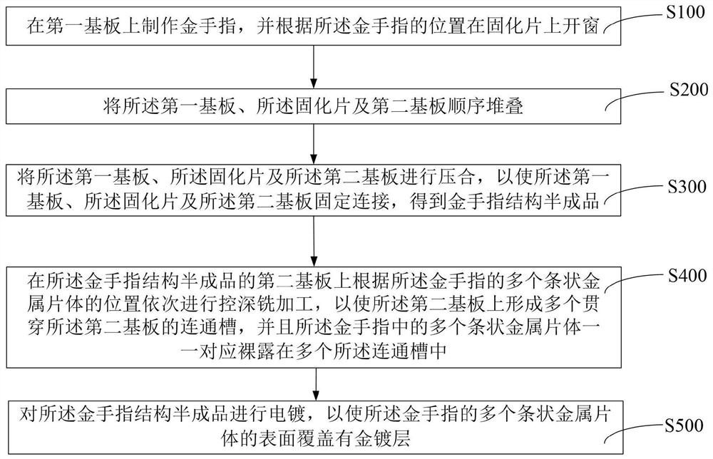
The present application provides a gold finger circuit board processing method and a gold finger circuit board. The above-mentioned gold finger circuit board processing method includes the following steps: making a gold finger on the first substrate, and opening a window on the solidified sheet according to the position of the golden finger; sequentially stacking the first substrate, the solidified sheet, and the second substrate; The substrate, the solidified sheet and the second substrate are pressed together so that the first substrate, the solidified sheet and the second substrate are fixedly connected; according to the position of the gold finger, multiple times of controlled depth milling are performed on the second substrate to make the second substrate A plurality of communication grooves penetrating through the second substrate are formed. By performing multiple controlled depth milling on the second substrate, multiple strip-shaped metal strips are exposed in multiple communication grooves one by one. When external equipment or human hands are about to come into contact with the gold finger, it will block the connection of the connected grooves. The notch can prevent the surface of the gold finger from being damaged during processing, which will further affect the efficiency of information transmission.

Description

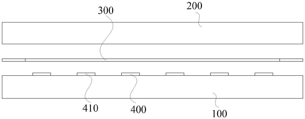
technical field [0001] The invention relates to the technical field of circuit boards, in particular to a processing method of a gold finger circuit board and a gold finger circuit board. Background technique [0002] Gold finger refers to the pads arranged like fingers that are inserted into the card slot and are in contact with the metal spring sheets in the card slot. A layer of nickel and a layer of gold will be plated on the surface of the pad, so it is commonly called gold finger. [0003] The traditional processing method of multi-layer circuit board gold finger is to make a gold finger contact piece on the surface of the inner layer board, and then stack the inner layer board, the solidified sheet and the outer layer board, and press them into a whole in a lamination machine, and finally put them on the outside. The layer board is slotted so that the gold fingers of the inner layer board can be connected to the outside through the groove body of the outer layer boar...

Claims


Application Information

Patent Timeline
Patent Type & Authority Patents(China)
IPC IPC(8): H05K3/00H05K3/18H05K3/40H05K3/46H05K1/02H05K1/11
CPCH05K3/00H05K3/188H05K3/403H05K3/46H05K1/117H05K1/0271H05K1/02
Inventor 许校彬
Owner HUAIAN TECHUANG TECH CO LTD
Learn More