Method for reducing contact resistance of through hole

A technology of contact resistance and barrier layer, which is applied in the manufacturing of circuits, electrical components, semiconductor/solid-state devices, etc., can solve the problems of increased contact resistance of through holes, affecting the quality of interconnect layers, and process interruption.

Pending Publication Date: 2021-05-04
SHANGHAI HUAHONG GRACE SEMICON MFG CORP
View PDF4 Cites 0 Cited by
  • Summary
  • Abstract
  • Description
  • Claims
  • Application Information

AI Technical Summary

Problems solved by technology

[0003] If the machine works abnormally and the process is interrupted, you must exit the machine and replace it to continue to complete the remaining process
If the interruption occurs when the metal barrier layer is just formed, the surface of the metal barrier layer will be oxidized when exiting the machine at this time, and an oxide layer will be formed on the surf

Method used


Image

  • Method for reducing contact resistance of through hole
  • Method for reducing contact resistance of through hole
  • Method for reducing contact resistance of through hole

Examples


Embodiment Construction

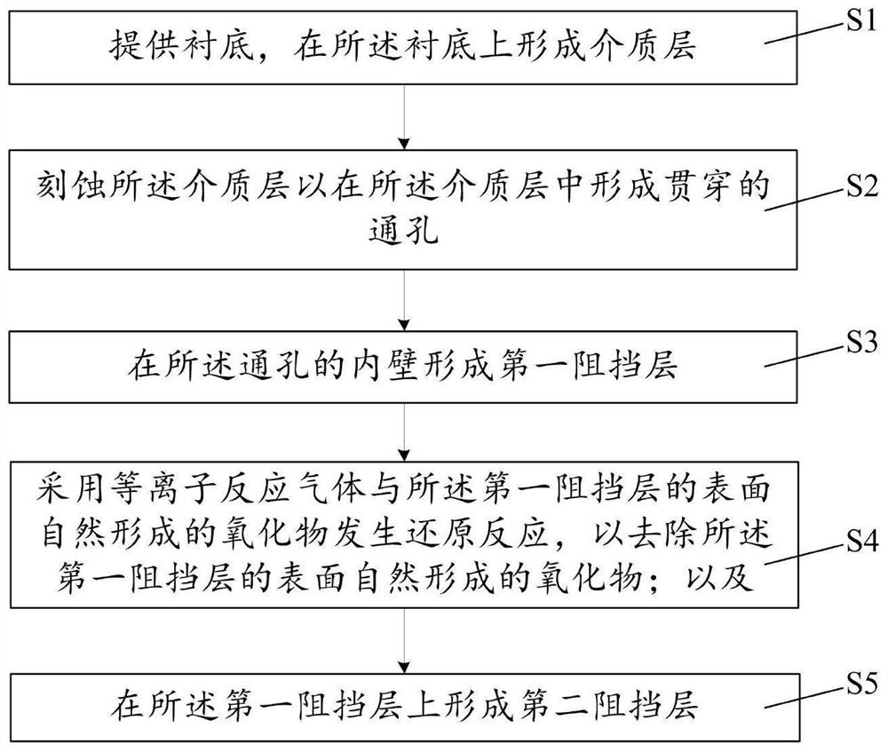
[0025] The specific implementation manner of the present invention will be described in more detail below with reference to schematic diagrams. The advantages and features of the present invention will be more apparent from the following description. It should be noted that all the drawings are in a very simplified form and use imprecise scales, and are only used to facilitate and clearly assist the purpose of illustrating the embodiments of the present invention.

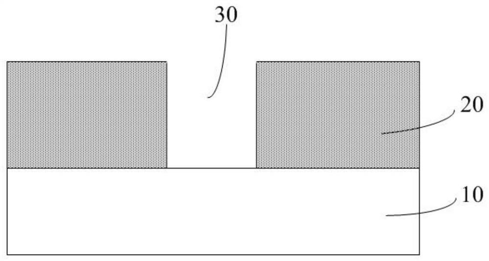
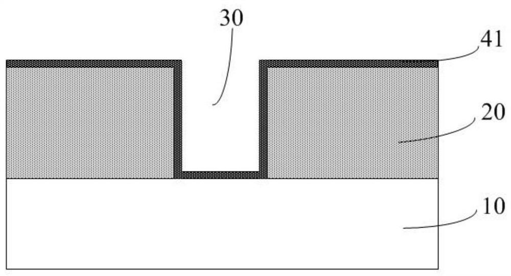
[0026] figure 1 The flow chart of the method for reducing the contact resistance of vias provided by this embodiment, Figure 2A-2C A schematic cross-sectional view of the corresponding steps of the method for reducing the contact resistance of the via provided in this embodiment. This embodiment provides a method for reducing the contact resistance of the through hole. The oxide naturally formed on the surface of the first barrier layer is removed by reducing the plasma reaction gas and the oxide naturally forme...


PUM

PropertyMeasurementUnit
Poweraaaaaaaaaa

Abstract

The invention provides a method for reducing contact resistance of a through hole, which comprises the following steps of: providing a substrate, and forming a dielectric layer on the substrate; etching the dielectric layer to form a through hole in the dielectric layer; forming a first barrier layer on the inner wall of the through hole; carrying out reduction reaction on plasma reaction gas and oxide naturally formed on the surface of the first barrier layer so as to remove the oxide naturally formed on the surface of the first barrier layer; and forming a second barrier layer on the first barrier layer; according to the invention, the plasma reaction gas and the oxide naturally formed on the surface of the first barrier layer are subjected to the reduction reaction to remove the oxide naturally formed on the surface of the first barrier layer, so that the contact resistance of the through hole can be reduced, and the connection quality of a through hole interconnection layer is ensured.

Description

technical field [0001] The invention relates to the technical field of semiconductors, in particular to a method for reducing the contact resistance of through holes. Background technique [0002] In the manufacture of semiconductor integrated circuits, multi-layer metallization technology has produced billions of metal vias, which usually use metal as a connection to form an electrical path between two layers of metal; on the other hand, contact vias The hole technology is also widely used in the connection between silicon devices and the first layer of metal. In the process of the metal barrier layer of the through-hole interconnection layer, it needs to be carried out under vacuum to avoid oxidation of the metal barrier layer by oxygen, which will cause the contact resistance of the through-hole to increase, and the increase in the contact resistance of the through-hole will affect the quality of the interconnection layer. In severe cases, an open circuit may occur. [...

Claims


Application Information

Patent Timeline
IPC IPC(8): H01L21/768
CPCH01L21/76831H01L21/76826H01L21/76802
Inventor 孙洪福公茂江姜国伟王雷
Owner SHANGHAI HUAHONG GRACE SEMICON MFG CORP
Why Eureka
Try Eureka