Circuit board impedance consistency control technology manufacturing method
A control technology and a manufacturing method are applied in the field of circuit board impedance consistency control technology, which can solve the problem of not fully considering impedance line design consistency, and achieve the effects of improving one-time yield, reducing costs and personnel costs.
- Summary
- Abstract
- Description
- Claims
- Application Information
AI Technical Summary
Problems solved by technology
Method used
Image
Examples
Embodiment 1
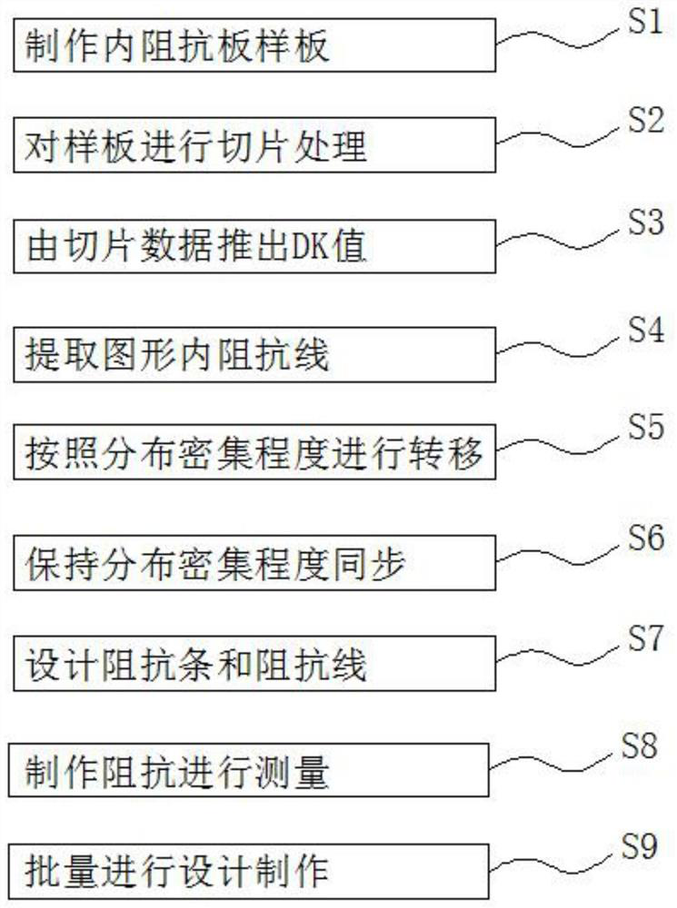
[0029] see figure 1 , a method for manufacturing circuit board impedance consistency control technology, comprising the following steps:
[0030] S1. Prefabricate the internal impedance board and make a batch of internal impedance board samples;
[0031] S2. Slicing the internal impedance plate template, and analyzing the sample data of the sliced sample of the internal impedance plate template;
[0032] S3. Summarize the sample data of the sliced samples to obtain the sliced data, and deduce the dielectric constant DK value of the internal impedance plate from the sliced data;
[0033] S4, using the dielectric constant DK value to extract the impedance line in the graph, and analyze the specific distribution of the impedance line in the graph;
[0034] S5. Transfer to the impedance bar according to the distribution density of the impedance line in the graph;
[0035] S6. According to the dielectric constant DK value of the internal impedance plate, the distribution...
Embodiment 2
[0046] see figure 2 , in the current manufacturing method of impedance design, when designing impedance strips and impedance lines, the design of impedance strips and impedance lines shows that the design consistency of impedance lines is not fully considered in separate design, so that the amount of line width bite is large when the impedance strip design line is etched to the copper space, resulting in impedance strips. The measured resistance value is too large, so we adopt the manufacturing method described in Example 1, including the following steps:
[0047] S1. Prefabricate the internal impedance board and make a batch of internal impedance board samples;
[0048] S2. Slicing the internal impedance plate template, and analyzing the sample data of the sliced sample of the internal impedance plate template;
[0049] S3. Summarize the sample data of the sliced samples to obtain the sliced data, and deduce the dielectric constant DK value of the internal impedance p...
Embodiment 3
[0064] see image 3 , in the current manufacturing method of impedance design, when designing impedance strips and impedance lines, the design consistency of the impedance line is not fully considered in the separate design. When the inner line to the copper design is intensively etched, the line width is normal and the resistance value is qualified. The design of the internal impedance line and the impedance line of the impedance strip lacks consistency. Therefore, we adopt the manufacturing method described in Embodiment 1, including the following steps: S1. Prefabricate the internal impedance plate and make a batch of internal impedance plate samples;
[0065] S2. Slicing the internal impedance plate template, and analyzing the sample data of the sliced sample of the internal impedance plate template;
[0066] S3. Summarize the sample data of the sliced samples to obtain the sliced data, and deduce the dielectric constant DK value of the internal impedance plate from ...
PUM
 Abstract
Description
Claims
Application Information


