
Post-processing technology of semiconductor carrier pcb circuit board

A PCB circuit board and post-processing technology, applied in the field of circuit board processing devices, can solve problems such as unsatisfactory cleaning effect

Active Publication Date: 2022-05-17
深圳市汇芯线路科技有限公司
View PDF0 Cites 0 Cited by
  • Summary
  • Abstract
  • Description
  • Claims
  • Application Information

AI Technical Summary

Problems solved by technology

[0005] Aiming at the deficiencies of the prior art, the present invention provides a semiconductor carrier PCB circuit board post-processing process, which has the advantages of easy removal of the circuit board, good cleaning effect, and low production cost, and solves the problem of unsatisfactory cleaning effect caused by manual clamping. question

Method used


Image

  • Post-processing technology of semiconductor carrier pcb circuit board
  • Post-processing technology of semiconductor carrier pcb circuit board
  • Post-processing technology of semiconductor carrier pcb circuit board

Examples


Embodiment Construction

[0034]The following will clearly and completely describe the technical solutions in the embodiments of the present invention with reference to the accompanying drawings in the embodiments of the present invention. Obviously, the described embodiments are only some, not all, embodiments of the present invention. Based on the embodiments of the present invention, all other embodiments obtained by persons of ordinary skill in the art without making creative efforts belong to the protection scope of the present invention.

[0035] As described in the background technology, there are deficiencies in the prior art. In order to solve the above technical problems, the application proposes a semiconductor carrier PCB circuit board post-processing technology

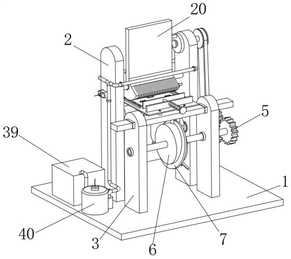
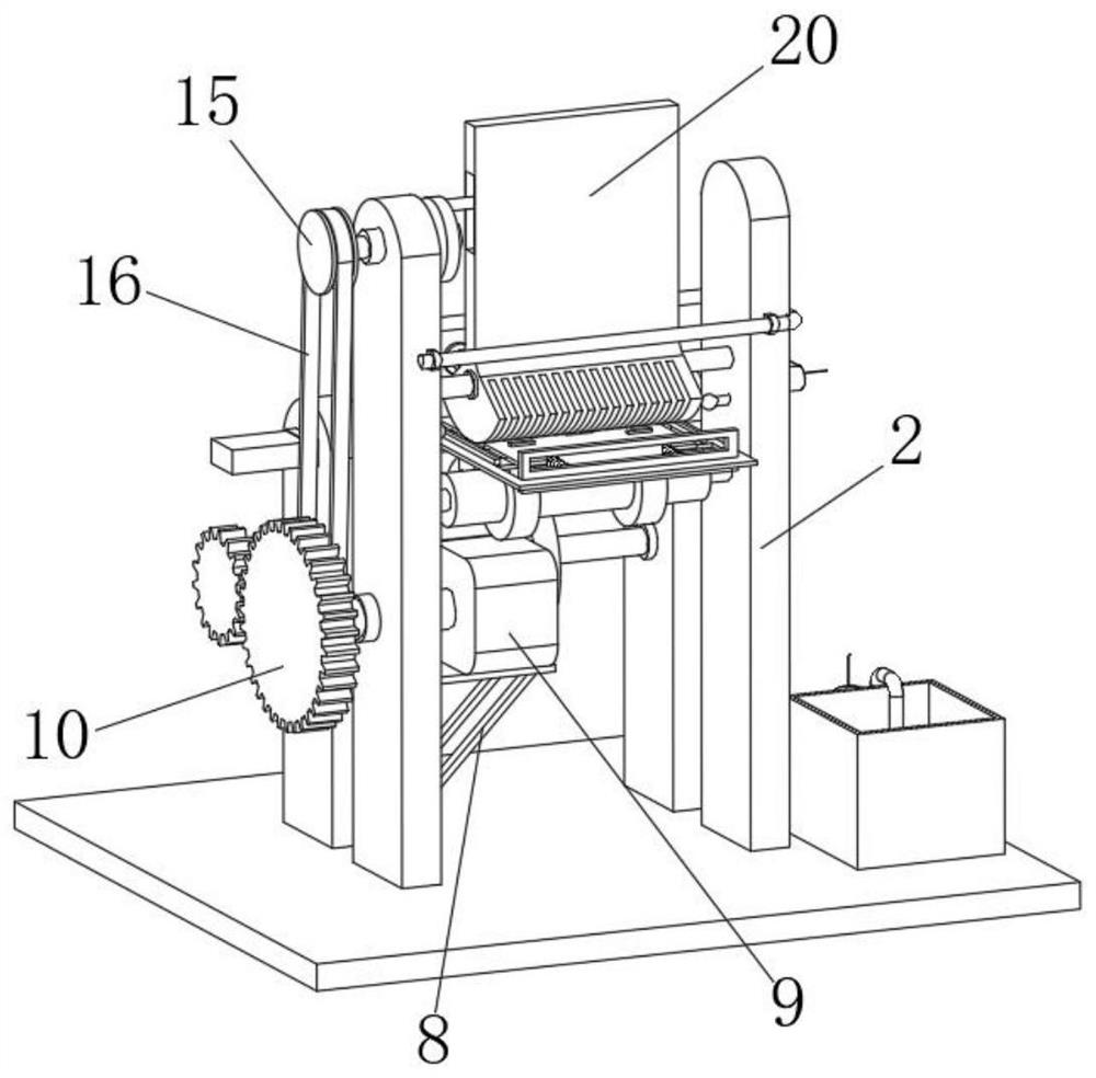
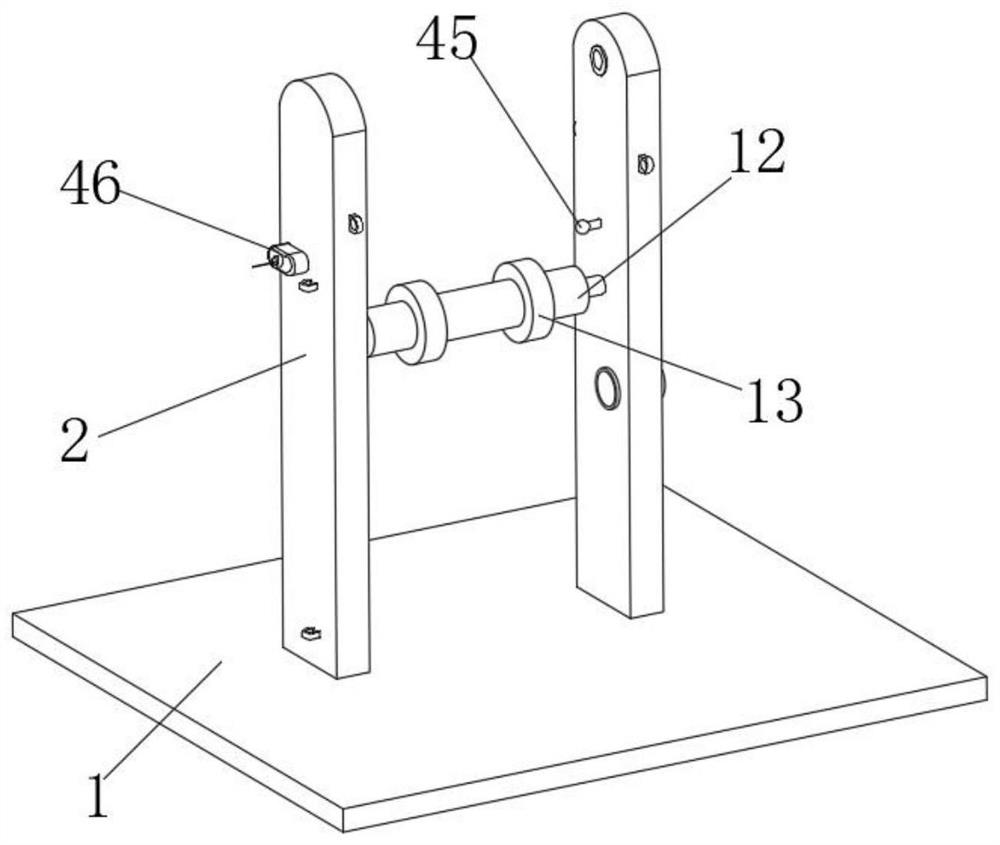
[0036] In a typical implementation of the present application, such as Figure 1-9 As shown, a semiconductor carrier PCB circuit board post-processing process, the process is completed by a semiconductor carrier PCB circuit board ...


PUM


Abstract

The invention relates to the technical field of circuit board processing devices, and discloses a semiconductor carrier PCB circuit board post-processing process. The output end of the driving motor 9 drives the input shaft through a coupling, and the input shaft makes the driving gear 10 rotate, and the driving gear 10 drives the phase The meshed driven gear 5 and the driving pulley 11 rotate, and the driven shaft 4 then drives the fixed wheel 6 and the inclined wheel 7 to rotate. When the inclined wheel 7 rotates, it contacts and collides with two small columns 23, so that the horizontal bar 22 is in the Slide in the horizontal direction in the sliding hole, so that the circuit board body 38 can be cleaned more thoroughly, the driving pulley 11 drives the driven pulley 15 to rotate through the transmission belt 16, the driven pulley 15 makes the control shaft 14 rotate, and the control shaft 14 further makes the control pulley 17 Rotation, the swinging block 20 is swung by the rotation of the rotating column 18, and the swinging block 20 drives the cleaning bristles 21 to clean the circuit board body 38, so that the circuit board body 38 can be cleaned from multiple angles.

Description

technical field [0001] The invention relates to the technical field of circuit board processing devices, in particular to a semiconductor carrier PCB circuit board post-processing process. Background technique [0002] The post-processing link of circuit board soldering is also very important. The so-called beginning and end, the previous work is only described for a certain type of device, and it cannot be grasped from the overall point of view. Only by doing a good job in this link In order to ensure the integrity of the circuit board soldering, the post-processing work of the circuit board mainly includes the following points: check the components according to the component list to ensure that all components are soldered in the correct position; confirm that the tantalum capacitor, diode, buzzer, tantalum Capacitors and other components with polarity requirements are soldered correctly; confirm that the pinout markings of integrated circuits, connectors and other multi-pi...

Claims


Application Information

Patent Timeline
Patent Type & Authority Patents(China)
IPC IPC(8): B08B1/00
CPCH05K3/26Y02P70/50
Inventor 付宝生付天龙
Owner 深圳市汇芯线路科技有限公司
Learn More