PCB CAF test module design method

A technology for testing modules and PCB boards, applied in the field of PCB board CAF testing module design, can solve problems such as adverse influencing factor analysis, short-circuit failure, poor insulation, etc., and achieve the effect of facilitating true cause analysis and screening.

Pending Publication Date: 2021-05-28
广州广合科技股份有限公司
View PDF0 Cites 1 Cited by
  • Summary
  • Abstract
  • Description
  • Claims
  • Application Information

AI Technical Summary

Problems solved by technology

When the PCB board is working in a high temperature and high humidity environment, the CAF phenomenon may occur between two insulated conductors, which will eventually lead to poor insulation and short circuit failure.
The CAF phenomenon may occur between the holes of the PCB board, between the holes and the inner and outer wires, and between the outer wires and the wires. In order to analyze the real cause of the CAF phenomenon on the PCB board, the commonly used CAF test module design , usually the connection between holes and holes, holes and inner and outer wires is designed together. Although the CAF test module design has a high degree of integration, it is not conducive to the analysis of influencing factors

Method used


Image

  • PCB CAF test module design method

Examples


Embodiment Construction

[0023] In order to enable those skilled in the art to better understand the solutions of the present invention, the following will clearly and completely describe the technical solutions in the embodiments of the present invention in conjunction with the drawings in the embodiments of the present invention. Obviously, the described embodiments are only It is an embodiment of a part of the present invention, but not all embodiments.

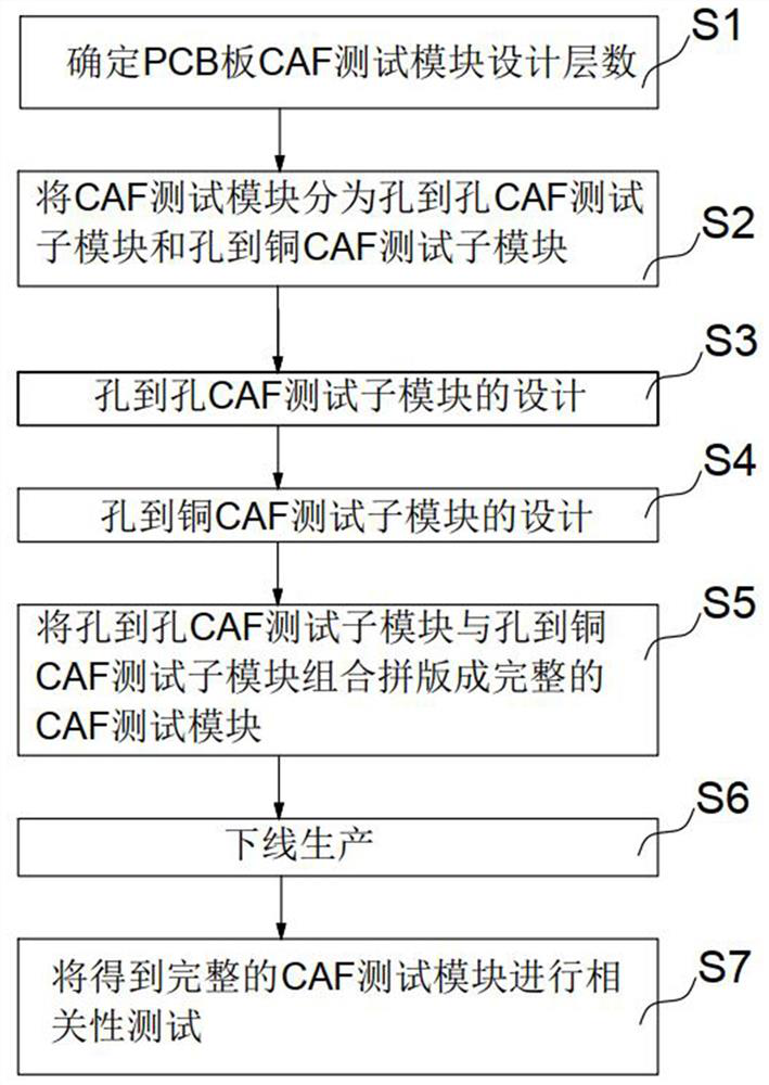
[0024] Such as figure 1 Shown, a kind of PCB board CAF test module design method of the present embodiment comprises the following steps:

[0025] S1. Determine the number of design layers of the PCB board CAF test module;

[0026] S2. The CAF test module is divided into a hole-to-hole CAF test sub-module and a hole-to-copper CAF test sub-module;

[0027] S3, the design of the hole-to-hole CAF test submodule: including the first inner layer graphic design and the first outer layer graphic design, the first inner layer graphic design includes the...


PUM


Abstract

The invention discloses a PCB CAF test module design method. The method comprises the steps that the number of designed layers of a PCB CAF test module is determined; the CAF test module is divided into a hole-to-hole CAF test sub-module and a hole-to-copper CAF test sub-module; the hole-to-hole CAF test sub-module is designed; the hole-to-copper CAF test sub-module is designed; and the hole-to-hole CAF test sub-module and the hole-to-copper CAF test sub-module are combined and spliced into a complete CAF test module, and testing is performed. The CAF test module is divided into the hole-to-hole CAF test sub-module and the hole-to-copper CAF test sub-module, the hole-to-hole CAF test sub-module can analyze CAF probabilities under different hole center-to-hole center distances and measure the influence proportion of drilling on CAF, and the hole-to-copper CAF test sub-module can analyze CAF probabilities under different hole center-to-hole center distances, and measures the influence proportion of the distances from different holes to the copper sheet, and the refined test module design is convenient for the true cause analysis of the CAF influence factors and is beneficial to the discrimination of primary and secondary factors.

Description

technical field [0001] The invention relates to the technical field of testing electronic components, in particular to a method for designing a PCB board CAF test module. Background technique [0002] As electronic products are increasingly miniaturized and highly integrated, the electronics industry has higher and higher requirements for the reliability of PCB boards. As one of the reliability testing items of PCB board, CAF testing has been paid more and more attention by the industry. CAF refers to the leakage of copper and copper salts that occurs during the migration of copper ions inside the PCB from the anode (high voltage) along the microcrack channel between glass fibers to the cathode (low voltage). When the PCB board is working in a high temperature and high humidity environment, the CAF phenomenon may occur between two insulated conductors, which will eventually lead to poor insulation and short circuit failure. The CAF phenomenon may occur between the holes of...

Claims


Application Information

Patent Timeline
Patent Type & Authority Applications(China)
IPC IPC(8): G01R31/28
CPCG01R31/2801
Inventor 章宏麦美环彭镜辉陈俊玲李春艳陈伟才
Owner 广州广合科技股份有限公司
Why Eureka
Try Eureka