Packaging design method and device of semiconductor chip

A design method and semiconductor technology, applied in computer-aided design, calculation, special data processing applications, etc., can solve the problem of large error in chip products and achieve the effect of reducing the error of chip products

Pending Publication Date: 2021-06-18
TELINK SEMICON SHANGHAI
View PDF6 Cites 2 Cited by
  • Summary
  • Abstract
  • Description
  • Claims
  • Application Information

AI Technical Summary

Problems solved by technology

However, the current LGA packaging design method cannot better adapt to the performance requirements of different products, resulting in large errors in the packaged chip products

Method used


Image

  • Packaging design method and device of semiconductor chip
  • Packaging design method and device of semiconductor chip
  • Packaging design method and device of semiconductor chip

Examples


Embodiment Construction

[0057] Exemplary embodiments of the present application are described below in conjunction with the accompanying drawings, which include various details of the embodiments of the present application to facilitate understanding, and they should be regarded as exemplary only. Accordingly, those of ordinary skill in the art will recognize that various changes and modifications of the embodiments described herein can be made without departing from the scope and spirit of the application. Also, descriptions of well-known functions and constructions are omitted in the following description for clarity and conciseness.

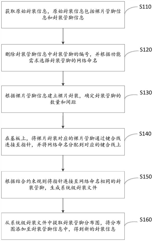
[0058] In a specific embodiment, such as figure 1 As shown, a packaging design method for a semiconductor chip is provided, comprising the steps of:

[0059] Step S110: Acquiring original packaging information, the original packaging information includes bare chip pin information and package pin information;

[0060] Step S120: Delete the number of the package pin ...


PUM


Abstract

The invention discloses a packaging design method and device of a semiconductor chip. According to the specific implementation scheme, the method comprises the following steps: acquiring original packaging information, wherein the original packaging information comprises bare chip pin information and packaging pin information; deleting the number of the packaging pin in the packaging pin information, and selecting the network name of the packaging pin according to the function requirement; establishing bare chip packaging according to the bare chip pin information, and determining the number and spacing of packaging pins; on the substrate, bare chip pins corresponding to bare chip packaging are connected to pointers through bonding wires, and network names are allocated to the corresponding bonding wires; connecting a pointer to a packaging pin with the same network name according to a combined constraint rule, and generating a system-level packaging file; and extracting the packaging pin distribution diagram from the system-level packaging file, and adding the distribution diagram into the packaging pin information to obtain new packaging information. The requirements of different product performances are met, and errors of chip products obtained through packaging are effectively reduced.

Description

technical field [0001] The present application relates to the field of semiconductor technology, in particular to the field of semiconductor package design. Background technique [0002] SIP (System In a Package) system-in-package technology uses a variety of bare chips or modules to arrange and assemble. If the arrangement is distinguished, it can be roughly divided into planar 2D packaging and 3D packaging structures. Among them, the LGA (landgrid array) grid array package, that is, the package with arrayed electrode contacts on the bottom surface, has become the best choice for high-density, high-performance, multi-pin packages such as CPUs and south / north bridge chips on motherboards. [0003] At present, the steps of the LGA packaging method include: obtaining original packaging data, establishing chip pins, determining chip orientation, setting chip layout and routing, and completing packaging. However, the current LGA packaging design method cannot better adapt to th...

Claims


Application Information

Patent Timeline
Patent Type & Authority Applications(China)
IPC IPC(8): G06F30/392
CPCG06F30/392
Inventor 梁文豪李翔
Owner TELINK SEMICON SHANGHAI
Why Eureka
Try Eureka