Device for reducing interference of USB (Universal Serial Bus) on antenna and terminal

Antenna interference and PCB board technology, applied in the direction of antenna, coupling device, antenna coupling, etc., can solve problems such as low USB transmission rate, antenna affecting standing wave, antenna standing wave ratio offset, etc., to improve user experience and product quality Effects on performance, protection of integrity

Pending Publication Date: 2021-06-18
ZTE CORP
View PDF0 Cites 0 Cited by
  • Summary
  • Abstract
  • Description
  • Claims
  • Application Information

AI Technical Summary

Problems solved by technology

[0002] The USB interface is an important interface of the terminal, which is used for charging and transmitting data. The traditional USB transmission rate is low, and the impact on the antenna is only the change of the antenna body after the USB interface is connected to the USB cable, which causes the VSWR of the antenna to shift. With the continuous improvement of the USB rate, after the USB cable is connected, it not only affects the standing wave of the antenna, but also generates interference, resulting in a serious decline in TIS (Total Isotropic Sensitivity, total omnidirectional sensitivity)

Method used


Image

  • Device for reducing interference of USB (Universal Serial Bus) on antenna and terminal
  • Device for reducing interference of USB (Universal Serial Bus) on antenna and terminal
  • Device for reducing interference of USB (Universal Serial Bus) on antenna and terminal

Examples


Embodiment 1

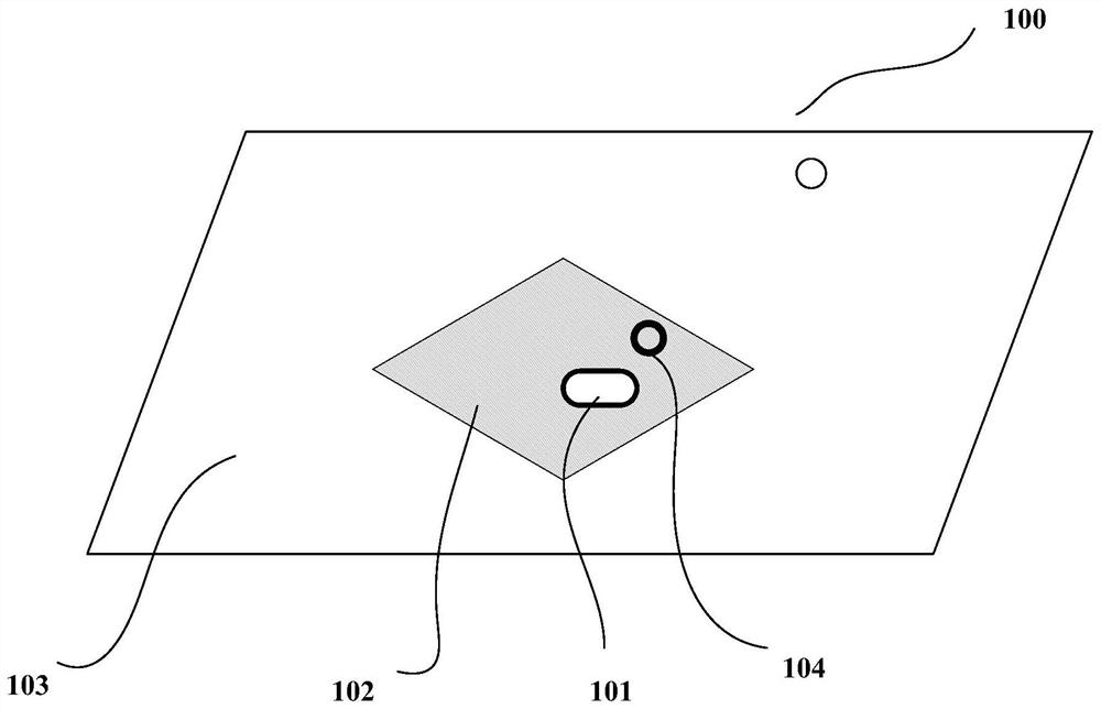
[0021] See figure 1 , A device 100 for reducing USB interference to antennas provided in this embodiment includes: a USB connector 101, a first interference reducing structure 102, and a PCB board 103;

[0022] The USB connector 101 is assembled in the area where the first interference reduction structure 102 is located;

[0023] The first interference reduction structure 102 is located on the surface layer of the surface layer board of the PCB board 103, and is used to isolate the ground of the ground shell of the USB connector 101 from the ground layer of the surface layer board;

[0024] The first IRI structure 102 further includes a first ground hole 104 through which the ground of the ground shell of the USB connector 101 is connected to the reference main ground of the PCB board 103 .

[0025] The device for reducing USB interference to antennas provided by the embodiments of the present invention can be applied to various mobile terminals, including but not limited to ...

Embodiment approach

[0081] The specific implementation method is as follows:

[0082] 1. The main board of the terminal equipment, that is, the PCB board, taking a 6-layer board as an example, (it can be any layer, it can be a first-order board, a second-order board, or any order board), top layer 71, second layer 72, third layer 73, Four layers, 74, five layers 75, bottom layer 76, 74 is selected as the reference main land, this embodiment uses 74 as the reference main land for example, the main board of the actual terminal product can select any layer of the PCB as the reference main land.

[0083] 2. Take the USB connector 701 on the top surface as an example. It should be noted that the USB connector 701 can also be on the bottom surface. The USB connector 701 can be USB TYPE-A, USB TYPE-B, USB MICRO-A, For USB connectors such as USB TYPE-C, the shell of the USB connector 701 is isolated from the ground of the top layer 71 through the second hollowed out position 705. The second hollowed out po...

Embodiment 2

[0094] This embodiment also provides a terminal, which includes the apparatus for reducing USB interference to an antenna in any one of the above embodiments.


PUM


Abstract

The invention provides a device for reducing interference of a USB (Universal Serial Bus) on an antenna and a terminal. The device comprises a USB connector, a first interference reducing structure and a PCB (Printed Circuit Board), wherein the USB connector is assembled in an area where the first interference reducing structure is located; the first interference reducing structure is positioned on the surface layer of a surface layer plate of the PCB and is used for isolating the ground of a grounding shell of the USB connector from the ground of the surface layer plate; and the first interference reducing structure further comprises a first grounding hole, wherein the ground of the grounding shell of the USB connector is connected to the reference main ground of the PCB through the first grounding hole. The invention further provides the terminal. The first interference reducing structure is arranged, the shell of the USB connector is independently isolated on the surface layer where the USB connector is located, and the shell is directly connected to the reference main ground of the main ground layer, so that the completeness of USB signals can be protected, interference generated in the USB data transmission process can be effectively restrained, the user experience can be effectively improved, and the product performance is improved.

Description

technical field [0001] Embodiments of the present invention relate to but are not limited to the field of computer communication networks, and in particular, relate to but are not limited to a device and terminal for reducing USB interference to antennas. Background technique [0002] The USB interface is an important interface of the terminal, which is used for charging and transmitting data. The traditional USB transmission rate is low, and the impact on the antenna is only the change of the antenna body after the USB interface is connected to the USB cable, which causes the VSWR of the antenna to shift. With the continuous improvement of the USB rate, after the USB cable is connected, it not only affects the standing wave of the antenna, but also generates interference, resulting in a serious decline in TIS (Total Isotropic Sensitivity, total omnidirectional sensitivity). Contents of the invention [0003] The embodiment of the present invention provides a device and te...

Claims


Application Information

Patent Timeline
IPC IPC(8): H01Q1/52H01Q1/50H01R12/71H01R13/648
CPCH01Q1/50H01Q1/52H01Q1/526H01R12/716H01R13/648H01R2201/02H01R12/71
Inventor 刘婷高明泉孙玮
Owner ZTE CORP
Why Eureka
Try Eureka