Electrostatic chuck with charge dissipation coating
An electrostatic chuck and coating technology, applied in the direction of holding devices, circuits, and manufacturing tools that apply electrostatic attraction, can solve problems such as damage to sharp edges and limited utility
- Summary
- Abstract
- Description
- Claims
- Application Information
AI Technical Summary
Benefits of technology
Problems solved by technology
Method used
Image

Examples
Embodiment Construction
[0016] Various example implementations of novel wafer substrate unchucking structures that provide electrostatic chucks and methods for using this configuration to reduce charge buildup that cause wafer substrates to "stick" after the electrostatic chuck has been powered down are described below. example. Localized surface charges can lead to unintended wafer clamping even in the absence of an external voltage. Therefore, there is also a need for improved platen or chuck configurations that control charge buildup in electrostatic chucks.
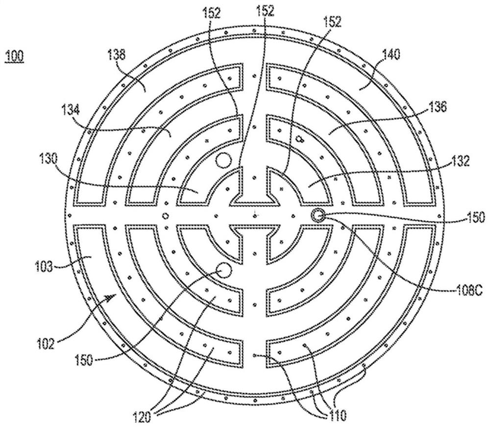
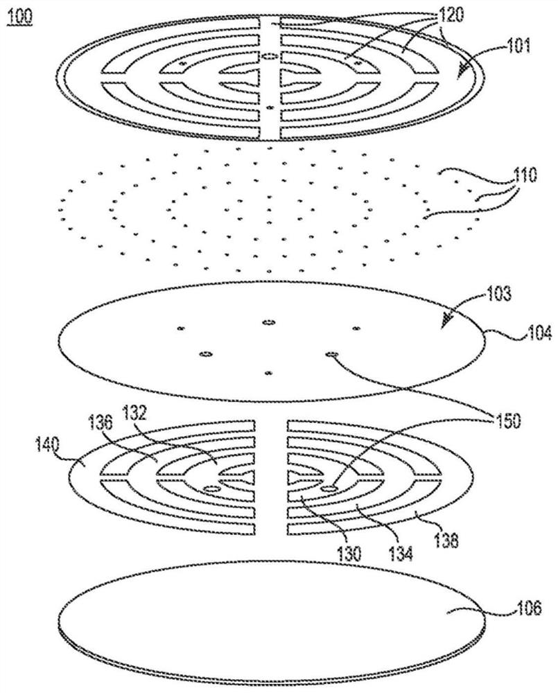
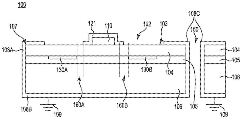
[0017] Referring now to the figures, figure 1 and 2 are top and exploded views, respectively, of an electrostatic chuck 100 designed to reduce wafer substrate "sticking" (increased from The difficulty with which the electrostatic chuck removes the wafer substrate) in order to "unclamp" or unclamp the wafer substrate from the electrostatic chuck after wafer substrate processing. Embodiments disclosed herein provide a conductive path on ra...
PUM
 Abstract
Description
Claims
Application Information