Dual-port PCIe SSD link fault tolerance device and method

A dual-port and link technology, which is applied in the field of computer communication, can solve the problems of time-lag data insecurity caused by the error processing of the upper-level business end, and achieve the effect of ensuring safety and realizing switching

Active Publication Date: 2021-07-13
SHANDONG SINOCHIP SEMICON
View PDF7 Cites 3 Cited by
  • Summary
  • Abstract
  • Description
  • Claims
  • Application Information

AI Technical Summary

Problems solved by technology

Common fault handling solutions mostly rely on the implementation of the host computer, and SSDs can only passively recei

Method used


Image

  • Dual-port PCIe SSD link fault tolerance device and method
  • Dual-port PCIe SSD link fault tolerance device and method

Examples


Embodiment 1

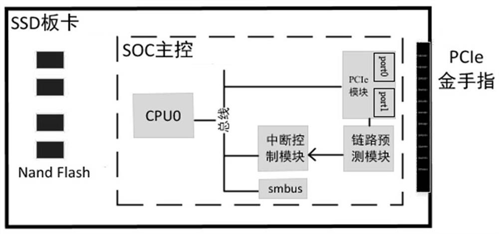
[0025] This embodiment discloses a dual-port PCIe SSD link fault-tolerant device. The device is implemented inside the SSD main control chip to realize active prediction of the SSD link state. Such as figure 1 As shown, the SSD board includes a SOC main control chip, nand flash, and PCIe golden finger interface. The SSD main control chip integrates the dual-port PCIe SSD fault-tolerant device described in this embodiment.

[0026] The dual-port PCIe SSD link fault-tolerant device in this embodiment includes a dual-port enabling unit, a link prediction logic unit, an interrupt control unit, and an smbus master-slave device.

[0027] The dual-port enable unit enables the dual-port mode of PCIe through the configuration register. All data channels are divided into two groups on average, each group is a port, and each group transmits data independently without being affected by the other channel. The effect of multiple hosts accessing the SSD can be realized through the PCIe swi...

Embodiment 2

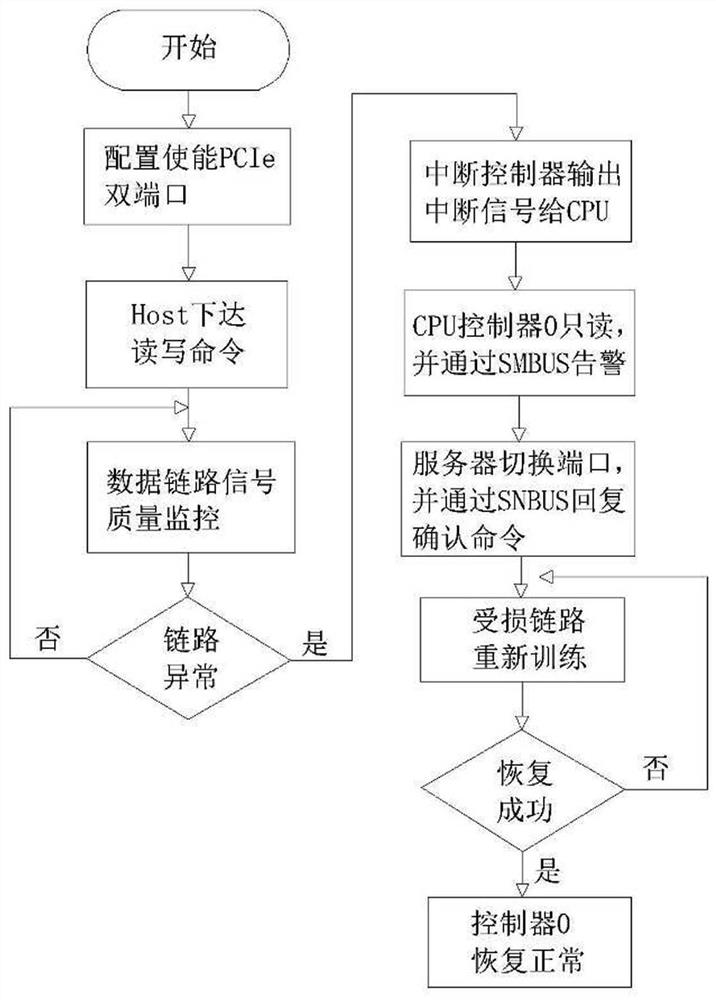
[0034] This embodiment discloses a dual-port PCIe SSD link fault-tolerant method. This method is implemented inside the SSD main control chip to realize active prediction of the SSD link state, such as figure 2 shown, including the following steps:

[0035]S01), the SSD firmware enables the current working mode to be the dual-port mode by configuring the register of the dual-port enabling unit. After the server is inserted, link training and negotiation are performed at both ends of the link to make the SSD work in the dual-port mode;

[0036] S02), during the normal reading and writing process of SSD, the link prediction logic unit is automatically in the running state. When the data packet received by the SSD has an ECRC or LCRC error, the bit error rate error statistics are started. When the bit error rate exceeds the threshold, it is identified as The link is abnormal, and the judgment result is output to the interrupt control unit;

[0037] S03), the interrupt control u...


PUM


Abstract

The invention discloses a dual-port PCIe SSD link fault tolerance device and method. The fault tolerance device comprises a dual-port enabling unit, a link prediction logic unit, an interrupt control unit and smbus master and slave equipment. The dual-port enabling unit enables a dual-port mode of PCIe through a configuration register, the link prediction logic unit is used for realizing evaluation of a link state, and the interrupt control unit takes output of the link prediction logic unit as an input signal and sends different interrupt request vector signals to a CPU through an internal bus according to different input results, an exception handling program of the firmware is triggered. The Smbus master and slave devices serve as out-of-band management interfaces and are used for sending device fault requests to the server out-of-band management controller and receiving out-of-band management commands. According to the method and the system, the active prediction of the link state by the SSD is realized, the error early warning is configured according to the stable state of the link, the switching of the standby port is realized, and the security of data accessed by the SSD is ensured.

Description

technical field [0001] The invention relates to the field of computer communication, in particular to a dual-port PCIe SSD link fault-tolerant device and method. Background technique [0002] With the popularization of cloud computing and big data applications, servers have higher and higher requirements for storage disk performance. SSDs based on PCIe interfaces are gradually replacing mechanical disks and SSDs with SATA interfaces. The remarkable feature of the PCIe interface is that it is faster, and the single-lane Gen4 PCIe interface has reached 16GT / s. However, there will be signal attenuation and interference when high-speed signals are transmitted on the data channel. When the data reaches the receiving end, it will bring challenges to the restoration of the original digital signal. In order to ensure the quality of the signal at the receiving end, the PCIe protocol stipulates that link equalizers are used at the sending end and receiving end of the physical layer t...

Claims


Application Information

Patent Timeline
IPC IPC(8): H04L12/939H04L12/935H04L12/703H04L12/711H04L12/721H04L45/247H04L45/28H04L49/111
CPCH04L49/552H04L49/555H04L49/557H04L49/30H04L45/28H04L45/22H04L45/70
Inventor 吴斌孙中琳段好强乔子龙
Owner SHANDONG SINOCHIP SEMICON
Why Eureka
Try Eureka