Electronic product welding method

A welding method and technology for electronic products, applied in welding equipment, electric heating devices, manufacturing tools, etc., can solve the problems of soldering pads, soldering inside soldering pads, reducing the yield of electronic products, etc. The effect of product defect rate

Active Publication Date: 2021-07-23
KUNSHAN LIANTAO ELECTRONICS CO LTD
View PDF10 Cites 0 Cited by
  • Summary
  • Abstract
  • Description
  • Claims
  • Application Information

AI Technical Summary

Problems solved by technology

Since the temperature at each solder pad is not the same, some solder pads have a problem of virtual soldering due to the incomplete melting of the solder paste, and it is easy to cause internal tin connection problems in some solder pads, which leads to the appearance of the connection between PCBA and FPCB. Bad and poorly functioning, reducing the yield of electronics

Method used


Image

  • Electronic product welding method
  • Electronic product welding method
  • Electronic product welding method

Examples


Embodiment Construction

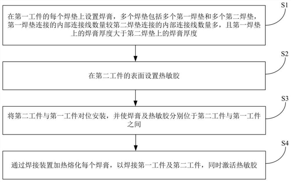
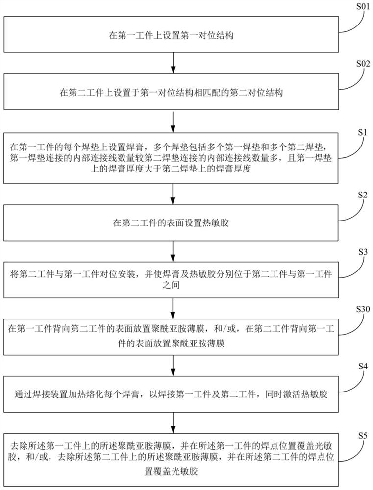
[0035] In order to make the technical problems solved by the present invention, the technical solutions adopted and the technical effects achieved clearer, the technical solutions of the present invention will be further described below in conjunction with the accompanying drawings and through specific implementation methods. It should be understood that the specific embodiments described here are only used to explain the present invention, but not to limit the present invention. In addition, it should be noted that, for the convenience of description, only the parts related to the present invention are shown in the drawings but not all of them.

[0036] In the description of the present invention, it should be noted that the terms "center", "upper", "lower", "left", "right", "vertical", "horizontal", "inner", "outer" etc. The indicated orientation or positional relationship is based on the orientation or positional relationship shown in the drawings, and is only for the conve...


PUM

PropertyMeasurementUnit
thicknessaaaaaaaaaa
thicknessaaaaaaaaaa
thicknessaaaaaaaaaa

Abstract

The invention discloses an electronic product welding method, and belongs to the technical field of electronic product manufacturing. The electronic product welding method comprises the following steps that welding paste is arranged on each welding pad of a first workpiece, a plurality of welding pads comprise a plurality of first welding pads and a plurality of second welding pads, and the number of internal connecting wires connected with the first welding pads is greater than the number of internal connecting wires connected with the second welding pads; the thickness of the welding paste on the first welding pads is greater than that of the soldering paste on the second welding pads; thermosensitive glue is arranged on the surface of a second workpiece; the second workpiece and the first workpiece are installed in an aligned mode, and the welding paste and the thermosensitive glue are located between the second workpiece and the first workpiece; and each welding paste is heated and melted through a welding device so as to weld the first workpiece and the second workpiece, and meanwhile, the thermosensitive glue is activated. According to the electronic product welding method, the probability of pseudo soldering and tin connection can be reduced, the connection quality of the first workpiece and the second workpiece is ensured, the situation of poor functions is avoided, so that the yield of electronic products is improved.

Description

technical field [0001] The invention relates to the technical field of electronic product manufacturing, in particular to an electronic product welding method. Background technique [0002] In the assembly process of electronic products, there is a need to weld two components, such as the need to weld PCBA and FPCB, and the quality of welding directly affects the quality of electronic products. [0003] In the prior art, the PCBA and the FPCB are welded by hot-press soldering. As an example, PCBA and FPCB have 16 solder pads respectively. When soldering the two, first pre-apply solder paste on each solder pad on a component, then align the PCBA and FPCB, and make the two components The 16 welding pads are aligned one by one, followed by high temperature and high pressure welding. Specifically, in the prior art, when solder paste is provided on the solder pads, the thickness of the solder paste on each solder pad is 0.1 mm, and the 16 solder pads are arranged in an array. ...

Claims


Application Information

Patent Timeline
Patent Type & Authority Applications(China)
IPC IPC(8): B23K1/00B23K3/04
CPCB23K1/0008B23K3/04B23K2101/36
Inventor 张凡李博丁刚尤勇
Owner KUNSHAN LIANTAO ELECTRONICS CO LTD
Why Eureka
Try Eureka