Check patentability & draft patents in minutes with Patsnap Eureka AI!

Pin configuration method of MCU chip and MCU chip

A configuration method and chip tube technology, applied in the field of MCU chips, can solve the problems of wiring winding, long design cycle, and inability to directly apply, and achieve the effect of flexible application

Active Publication Date: 2021-08-17
无锡矽杰微电子有限公司 +1
View PDF14 Cites 0 Cited by
  • Summary
  • Abstract
  • Description
  • Claims
  • Application Information

AI Technical Summary

Problems solved by technology

[0003] First of all, if it is not easy to connect during board-level wiring, for example, an analog signal pin is above the chip, but the board-level analog signal pin can only be placed below the chip due to space constraints, then the wiring will be relatively convoluted. , resulting in too long traces, which increases noise;
[0004] Secondly, after the wiring is determined at the board level, if the usage requirements change, the wiring of the corresponding pin pins will change, and at this time, the board can only be re-arranged;
[0005] In addition, it is necessary to re-layout the board when there is a mistake in the board-level wiring;
[0006] Finally, due to the update and upgrade of the MCU, when the MCU chip on the circuit board is replaced, the new MCU cannot be directly applied to the circuit board due to the different definitions of the function pins of different MCUs, and the circuit board needs to be redesigned, and the circuit board needs to be redesigned. Board re-layout results in longer design cycles and higher costs

Method used


Image

  • Pin configuration method of MCU chip and MCU chip
  • Pin configuration method of MCU chip and MCU chip
  • Pin configuration method of MCU chip and MCU chip

Examples


Embodiment 2

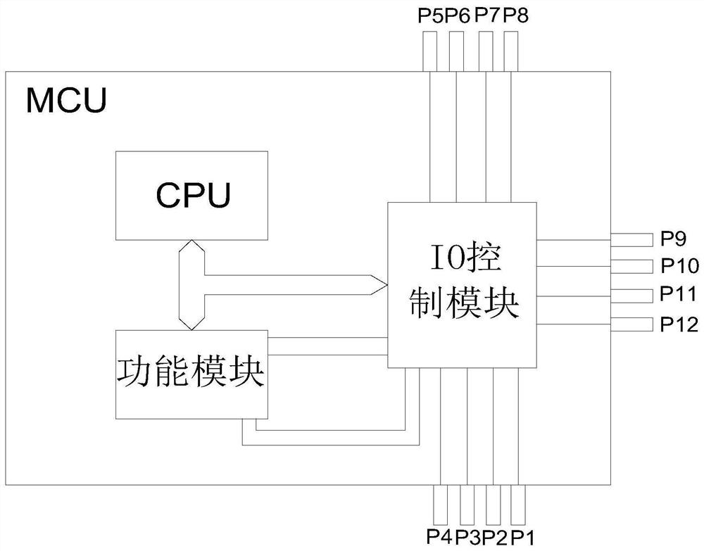
[0034] Such as Figure 1-3 As shown, taking the MCU chip of twelve functional pins as an example, the steps of the method of the present invention during actual implementation are as follows:

[0035] A: When designing the MCU chip, except for the power pins, ground pins and clock pins that have been determined as PINs, the 12 functional pins do not define specific functions for the time being. On the functional module inside the chip;

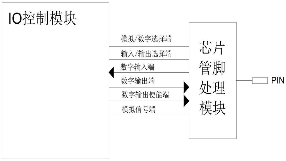
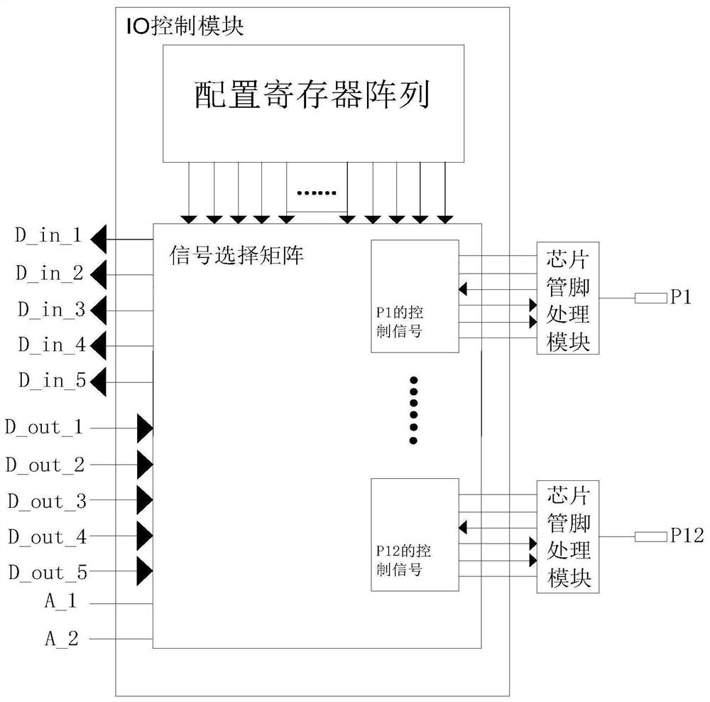
[0036] B: Let the 12 functional pins be connected to different chip pin processing modules, the working mode of each chip pin processing module can be configured, and the internal signal pins of each chip pin processing module are connected to the MCU chip On the I / O control module, the signal connection diagram between a single functional pin and the corresponding chip pin processing module can be referred to figure 2 ;

[0037] C: The chip pin processing module defaults to the digital input mode, so that the function pin connected to the...


PUM


Abstract

The invention relates to the technical field of chip design, and discloses a pin configuration method of an MCU chip and the MCU chip. In the method, a power supply pin, a grounding pin and a clock pin of the MCU chip are directly and electrically connected with a power supply end, a grounding end and a clock end of a CPU of the MCU chip, and an IO pin of the MCU chip is electrically connected with the CPU through an IO control module. In actual use, the working mode of the IO pin is configured through the IO control module, so that more wiring on the PCB due to limitation of the spatial position of the IO pin is not needed, and board rearrangement due to change of use requirements or wrong connection between a peripheral circuit on the PCB and the IO pin of the MCU chip is not needed; the PCB does not need to be re-typeset when the MCU chip is upgraded and replaced, and only the working mode of the I-O pin of the MCU chip needs to be set to be the same as the working mode of the I-O pin of the original MCU chip on the PCB, so that the method is simple and convenient, and a customer can flexibly apply the method according to own requirements.

Description

technical field [0001] The invention relates to the technical field of chip design, in particular to a pin configuration method of an MCU chip and the MCU chip. Background technique [0002] MCU, also known as single-chip microcomputer, is to appropriately reduce the frequency and specifications of the central processing unit, and integrate functional modules such as memory, counter, USB, A / D conversion, UART, PLC, DMA, PWM, middle segment, and even LCD drive circuits. On a single chip, a chip-level computer is formed to control different combinations for different applications. At present, after the design of the MCU chip is completed, the function of each pin of the chip is basically determined. However, in actual use, the following conditions will affect the layout position of the functional pins of the MCU chip: [0003] First of all, if it is not easy to connect during board-level wiring, for example, an analog signal pin is above the chip, but the board-level analog s...

Claims


Application Information

Patent Timeline
IPC IPC(8): G05B19/042
CPCG05B19/0423G05B2219/25257
Inventor 刘建湘
Owner 无锡矽杰微电子有限公司
Features
  • R&D
  • Intellectual Property
  • Life Sciences
  • Materials
  • Tech Scout
  • Unparalleled Data Quality
  • Higher Quality Content
  • 60% Fewer Hallucinations
Learn More