
In-mold electronic touchpad and manufacturing method thereof

A manufacturing method and internal electronic technology, which are applied in the direction of electrical digital data processing, instruments, and data processing input/output processes, etc., can solve the problems of poor universal application environment, cracking and separation of connection positions, low flexibility, etc. The effect of assembly fault tolerance, improved connection strength, and improved wiring flexibility

Pending Publication Date: 2021-09-03
深圳市合盛创杰科技有限公司
View PDF0 Cites 0 Cited by
  • Summary
  • Abstract
  • Description
  • Claims
  • Application Information

AI Technical Summary

Problems solved by technology

[0003] The touch film on the in-mold electronic panel is usually a composite film made of PC and PMMA. This kind of composite film has poor flexibility and brittle texture, and the composite film can only be connected to the FPC at the edge, so it is difficult to insert When unplugging and assembling or working in an environment with a large amount of vibration, the FPC can easily drive the touch film to shift, resulting in cracking and separation at the connection position between the two, and the brittle touch film may also be disconnected. ; Assembly error tolerance rate is low, and application environment universality is poor
[0004] At the same time, in the process of re-arranging the FPC after installing the in-mold electronic panel, in order to prevent the touch film from being damaged due to the excessive range of movement of the FPC, the routing of the FPC can only be adjusted in a small range, which is flexible. low level

Method used


Image

  • In-mold electronic touchpad and manufacturing method thereof
  • In-mold electronic touchpad and manufacturing method thereof
  • In-mold electronic touchpad and manufacturing method thereof

Examples


Embodiment Construction

[0031] In order to understand the technical features, objects and effects of the present invention, specific embodiments of the present invention will be described in detail with reference to the accompanying drawings.

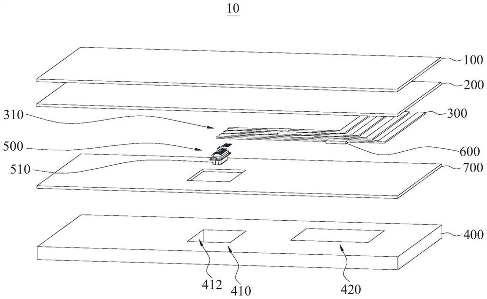
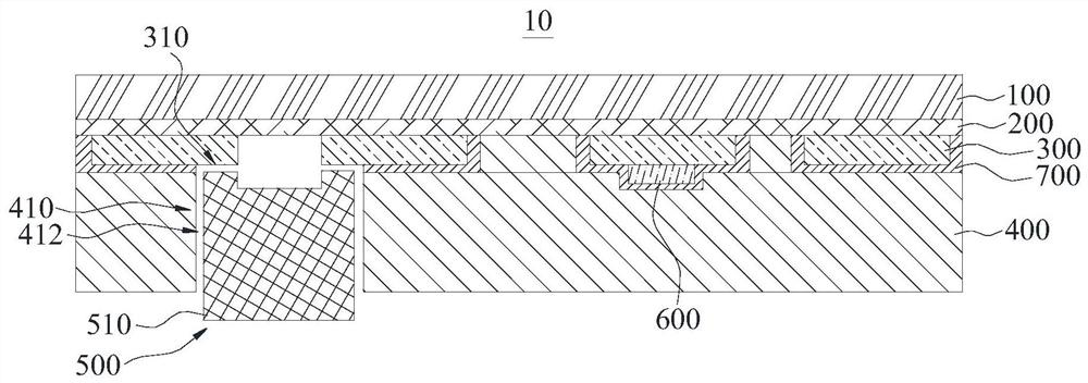
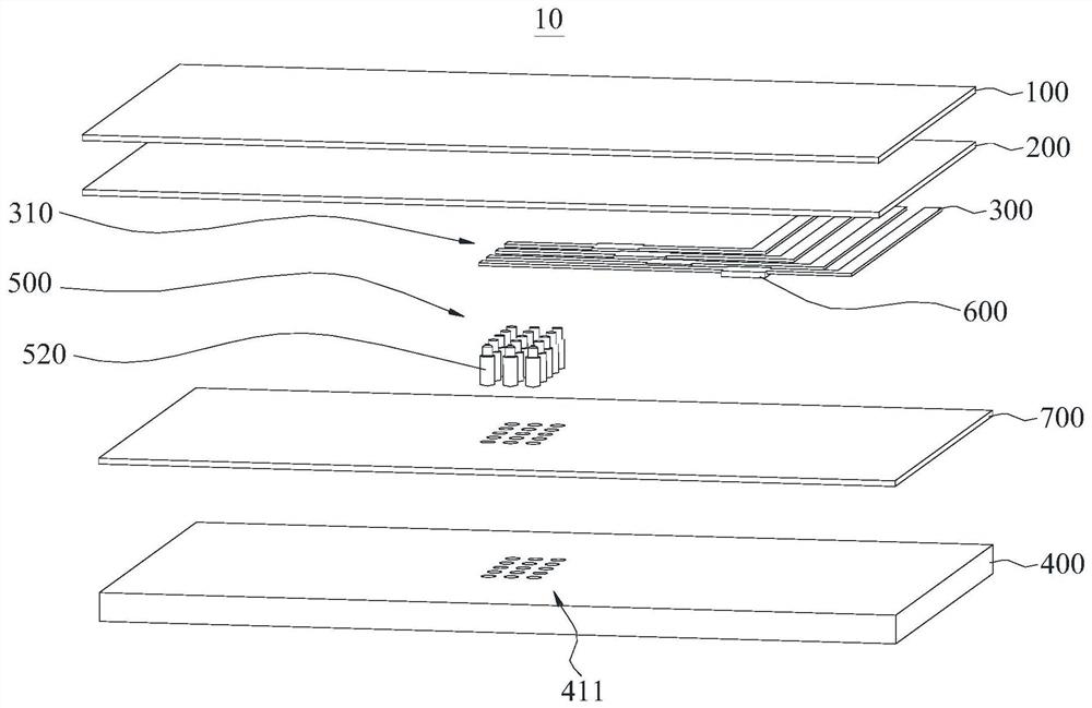
[0032] figure 1 An in-mold electronic touch panel 10 in some embodiments of the present invention is shown. image 3 An in-one electronic touch plate 10 in some embodiments of the present invention is shown, which is connected to the external controller, which functions as an external controller. The mode electron touch panel 10 includes a base film layer 100, a pattern layer 200, a line layer 300, an injection molding member 400, and a connecting member 500. The pattern layer 200 is disposed on the lower surface of the base film layer 100, which facilitates the function of each location of the user to identify the in-mold electronic touch panel 10. The line layer 300 is disposed on the lower surface of the base film layer 100, and the portion of the line layer 30...


PUM


Abstract

The invention discloses an in-mold electronic touchpad, and the touchpad comprises a base film layer, a pattern layer, a circuit layer, an injection molding part and a connecting part; the pattern layer is arranged on the lower surface of the base film layer, the circuit layer is arranged on the lower surface of the base film layer, part of the circuit layer covers the pattern layer, and an external connection end is arranged on the circuit layer; the injection molding part (400) is provided with a clearance position, the injection molding part is arranged on the lower surface of the base film layer, the injection molding part covers the pattern layer and the circuit layer, the external connection end is exposed in the clearance position, and the connection part is connected with the external connection end; according to the in-mold electronic touchpad, the connecting part is arranged to replace an FPC, so the external connecting end of the circuit layer can be flexibly arranged at the position, away from the edge, of the base film layer; compared with the edge position, the periphery of the external connecting end can be connected with the base film layer, the connecting strength between the external connecting end and the base film layer is improved, and the assembling error-tolerant rate of the in-mold electronic touchpad is increased; secondly, the connecting part is connected with the external controller, so that the wiring flexibility of the in-mold electronic touchpad is improved.

Description

Technical field [0001] The present invention relates to the field of in-mold electron touch panels, and more particularly to an in-mold electron touch panel and a method of fabricating it. Background technique [0002] The mode electronic panel is widely used in various fields due to its advantages of lightness and highest degree of beauty, but existing modular electronic panels still have the following technical issues in actual production and use: [0003] The touch film on the molded electronic panel is typically a composite film made of PC and PMMA. The flexibility of such composite film is poor, and the texture is almost, and the composite film can only be connected to the FPC at the edge position, so inserted When the unit is inserted or in the environment where the vibration is large, the FPC can easily drive the touch film offset, resulting in the connection of the two connected positions, and the touch film of the texture is likely to have a circuit. The assembled fault ...

Claims


Application Information

Patent Timeline
Patent Type & Authority Applications(China)
IPC IPC(8): G06F3/0354
CPCG06F3/03547
Inventor 艾建华王三刚
Owner 深圳市合盛创杰科技有限公司
Learn More