A helical waveguide grating assisted reverse coupler type optical dispersion delay line

A reverse coupler and helicon wave technology, applied in the field of optical communication, can solve the problems of increasing system complexity, increasing integration difficulty, unfavorable miniaturization, etc., achieving low transmission loss, low insertion loss, and suppression of output spectral side lobes Effect

Active Publication Date: 2021-11-05
SOUTHEAST UNIV
View PDF8 Cites 0 Cited by
  • Summary
  • Abstract
  • Description
  • Claims
  • Application Information

AI Technical Summary

Problems solved by technology

Among them, the microring resonator and photonic crystal waveguide are affected by the high insertion loss of the device itself, so it is difficult to be practical in the actual photonic chip; when the single-waveguide Bragg chirped grating adopts a spiral on-chip layout, it can be realized in a small device size. Larger total delay and high dispersion value, however, this reflective dispersion delay line requires an external independent circulator or an on-chip optical splitter to convert it into a two-port device in order to separate the reflected signal, the former will increase the system The complexity is not conducive to miniaturization, and the latter will introduce an additional 3dB insertion loss; another dispersion delay line based on a grating-assisted reverse coupler cleverly uses a double waveguide structure to replace a single waveguide with a reverse coupling The reflective output mode of the grating effectively solves the separation problem of the output signal. However, the need for a large dispersion value inevitably requires an increase in the length of the reverse coupling region of the device, which greatly increases the difficulty of integration under the limited chip size.

Method used


Image

  • A helical waveguide grating assisted reverse coupler type optical dispersion delay line
  • A helical waveguide grating assisted reverse coupler type optical dispersion delay line
  • A helical waveguide grating assisted reverse coupler type optical dispersion delay line

Examples


Embodiment 1

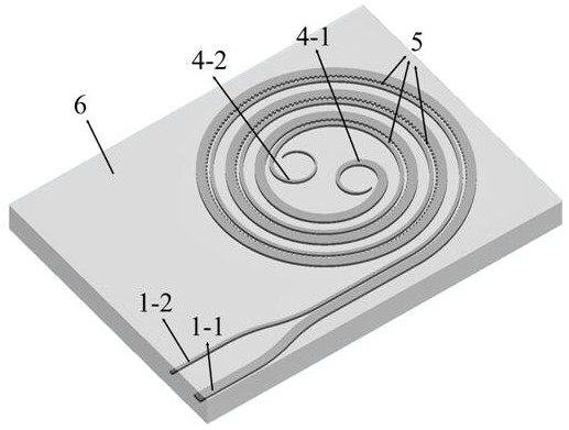
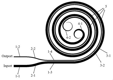
[0020] Embodiment 1: see figure 1 , a helical waveguide grating assisted reverse coupler type optical dispersion delay line, including SiO 2 Cladding 6, SiO 2There is a waveguide layer arranged horizontally inside the cladding, and the waveguide layer is made of Si material, including four transverse straight waveguides, namely the first straight waveguide 1-1, the second straight waveguide 1-2, and the third straight waveguide 1 -3. The fourth straight waveguide 1-4, two S-shaped curved waveguides, that is, the first S-shaped curved waveguide 2-1, the second S-shaped curved waveguide 2-2, two sections of spiral loss lines, that is, the first spiral loss line 4 -1. The second helical loss line 4-2, and a section of helical waveguide chirped grating assisted reverse coupler; where a transverse wide straight waveguide on the left is used as the input end of the reverse coupler, and a transverse narrow straight waveguide is used as the reverse coupling The two ports are connect...

Embodiment 2

[0021] Embodiment 2: refer to figure 1 — Figure 4 ,Such as figure 1 and figure 2 As shown, the present invention designs a spiral waveguide grating assisted reverse coupler type optical dispersion delay line, and its waveguide layer is embedded in SiO 2 The strip-shaped Si waveguide in the cladding 6 includes a first straight waveguide 1-1, a second straight waveguide 1-2, a first S-shaped curved waveguide 2-1, a second S-shaped curved waveguide 2-2, and a first spiral Loss line 4-1, second helical loss line 4-2 and helical waveguide chirped grating assisted reverse coupler 5. The left ends of the first straight waveguide 1-1 and the second straight waveguide 1-2 are respectively the input port (Inport) and the output port (Outport) of the dispersion delay line; the third straight waveguide 1-3 and the fourth straight waveguide 1 -4 is used as a pre-buffer, the right end is respectively connected to the left end of the spiral single-side wall modulation waveguide grating...


PUM

PropertyMeasurementUnit
thicknessaaaaaaaaaa

Abstract

The invention relates to a spiral waveguide grating assisted reverse coupler type optical dispersion delay line, comprising SiO 2 Cladding, SiO 2 There is a horizontally arranged waveguide layer inside the cladding, and the waveguide layer is made of Si material, including four transverse straight waveguides, two S-shaped curved waveguides, two spiral loss lines, and a spiral waveguide chirped grating-assisted inversion Coupler; where a horizontal wide straight waveguide on the left is used as the input end of the reverse coupler, and a horizontal narrow straight waveguide is used as the output end of the reverse coupler, and the two ports are connected to the reverse coupler through a pair of S-shaped curved waveguides; The left end of the first straight waveguide is the input port of the dispersion delay line, the left end of the second straight waveguide is the output port of the dispersion delay line; the third straight waveguide and the fourth straight waveguide are used as the pre-buffer, and the right end is respectively connected with the spiral single side wall The modulation waveguide grating is connected to the left end of the helical strip / taper waveguide.

Description

technical field [0001] The invention relates to a delay line, in particular to a spiral waveguide grating assisted reverse coupler type optical dispersion delay line, which belongs to the technical field of optical communication. Background technique [0002] With the rapid development of optical communication technology in the direction of high speed and large capacity, the requirements for efficiency and accuracy of information transmission and processing are getting higher and higher. Dispersion delay technology with large dispersion value has become the key to improving the performance of information systems. The optical dispersion delay line can make the output optical signal have a group delay that varies with the wavelength, and the delay value and wavelength generally conform to a linear change relationship, which can be applied to dispersion compensation, optical buffering, optical true delay network, and integrated microwave photonics. Signal generation and process...

Claims


Application Information

Patent Timeline
Patent Type & Authority Patents(China)
IPC IPC(8): G02B6/12G02B6/28
CPCG02B6/2861G02B6/12009
Inventor 胡国华汪冬宇邓春雨黄磊孙彧恽斌峰崔一平
Owner SOUTHEAST UNIV
Why Eureka
Try Eureka