Optical control terahertz wave amplitude modulator based on silicon nanoneedle

An amplitude modulation and terahertz wave technology, applied in the field of terahertz applications, can solve the problems of low power and large terahertz loss, and achieve the effect of large modulation depth and low insertion loss

Inactive Publication Date: 2016-08-31
UNIV OF ELECTRONICS SCI & TECH OF CHINA
View PDF5 Cites 14 Cited by
  • Summary
  • Abstract
  • Description
  • Claims
  • Application Information

AI Technical Summary

Problems solved by technology

However, the refractive index of silicon wafers is as high as 3.4. Whether laser or terahertz waves are incident on silicon wafers, serious reflections will occur. The reflection of terahertz waves reaches 35%-50%, and the reflection of lasers is as high as 40%. Therefore, the terahertz loss of the device is very large, and the terahertz transmittance of the high-resistance silicon chip spatial terahertz modulator reported above is only 50%, and the power of the terahertz radiation source is generally low at present (microwatts to several milliwatts) is particularly unfavorable; on the other hand, it is also necessary to provide greater laser power in order to obtain the terahertz modulation effect that meets the practical requirements

Method used


Image

  • Optical control terahertz wave amplitude modulator based on silicon nanoneedle
  • Optical control terahertz wave amplitude modulator based on silicon nanoneedle
  • Optical control terahertz wave amplitude modulator based on silicon nanoneedle

Examples


Embodiment Construction

[0023] The present invention will be described in further detail below in conjunction with the accompanying drawings and embodiments.

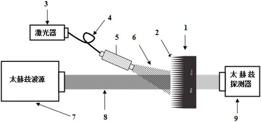
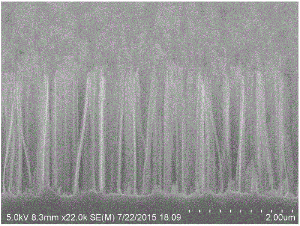
[0024] In this embodiment, an optically controlled terahertz wave modulator based on silicon nanoneedles is provided, and its structure is as follows figure 2 As shown, it includes a semiconductor laser 3, an optical fiber 4, an optical fiber modulator 5 and a terahertz amplitude modulation structure. The laser light generated by the semiconductor laser 3 is coupled into the optical fiber modulator 5 through an optical fiber 4; the terahertz amplitude modulation structure is made of silicon-based The bottom layer 1 and the silicon nano-tip array 2 on its surface are composed, and the optical fiber modulator outputs modulated laser light 6 incident on the surface of the silicon nano-tip array; thus, the terahertz wave beam 8 generated by the terahertz wave source 7 produces a transmission modulation effect, and is Received by Terahertz Wave De...


PUM


Abstract

The invention belongs to the field of terahertz imaging technologies, relates to a modulation device in the related field of terahertz imaging, and in particular provides an optical control terahertz wave amplitude modulator based on a silicon nanoneedle. The optical control terahertz wave amplitude modulator comprises a semiconductor laser, an optical fibre, an optical fibre modulator and a terahertz amplitude modulation structure; laser generated by the semiconductor laser enters the optical fibre modulator through optical fibre coupling; the optical control terahertz wave amplitude modulator is characterized in that the terahertz amplitude modulation structure is composed of a silicon-based bottom layer and a silicon nanoneedle tip array on the surface; and the optical fibre modulator outputs modulated laser incident to the surface of the silicon nanoneedle tip array. According to the optical control terahertz wave amplitude modulator disclosed by the invention, a dual-layer structure including the silicon nanoneedle tip array and a high-resistivity silicon/intrinsic silicon layer is adopted; the silicon nanoneedle tip array has the gradient change of a refractive index on the surface of high-resistivity silicon/intrinsic silicon; reflection of terahertz wave and pumping laser can be reduced simultaneously; the insertion loss of the device is obviously reduced; the pumping laser utilization rate is increased; and the device has relatively high modulation depth under relatively low pumping laser power.

Description

technical field [0001] The invention belongs to the technical field of terahertz applications, and relates to a signal amplitude modulation device in the related fields of terahertz imaging and communication, in particular to an optically controlled terahertz wave amplitude modulator based on silicon nano needles. Background technique [0002] Terahertz wave is an electromagnetic wave with a frequency between 0.1THz and 10THz; as a kind of electromagnetic wave, terahertz radiation can be used as a signal source for object imaging like visible light, X-rays, infrared, and ultrasonic waves. The principle is to use the imaging system to analyze and process the recorded transmission spectrum or reflection spectrum information (including the two-dimensional information of amplitude and phase) of the sample, and finally obtain the terahertz image of the sample. Terahertz imaging technology has become a hot spot and focus in the application of terahertz science and technology, and ...

Claims


Application Information

Patent Timeline
Patent Type & Authority Applications(China)
IPC IPC(8): H01S1/02
CPCH01S1/02
Inventor 文岐业刘浩天史中伟杨青慧文天龙陈智荆玉兰张怀武
Owner UNIV OF ELECTRONICS SCI & TECH OF CHINA
Why Eureka
Try Eureka